- 您現(xiàn)在的位置:買賣IC網(wǎng) > PDF目錄374277 > K4N51163QC-ZC33 (SAMSUNG SEMICONDUCTOR CO. LTD.) 512Mbit gDDR2 SDRAM PDF資料下載
參數(shù)資料
| 型號: | K4N51163QC-ZC33 |
| 廠商: | SAMSUNG SEMICONDUCTOR CO. LTD. |
| 英文描述: | 512Mbit gDDR2 SDRAM |
| 中文描述: | 512MB的GDDR2 SDRAM的 |
| 文件頁數(shù): | 14/64頁 |
| 文件大小: | 1420K |
| 代理商: | K4N51163QC-ZC33 |
第1頁第2頁第3頁第4頁第5頁第6頁第7頁第8頁第9頁第10頁第11頁第12頁第13頁當(dāng)前第14頁第15頁第16頁第17頁第18頁第19頁第20頁第21頁第22頁第23頁第24頁第25頁第26頁第27頁第28頁第29頁第30頁第31頁第32頁第33頁第34頁第35頁第36頁第37頁第38頁第39頁第40頁第41頁第42頁第43頁第44頁第45頁第46頁第47頁第48頁第49頁第50頁第51頁第52頁第53頁第54頁第55頁第56頁第57頁第58頁第59頁第60頁第61頁第62頁第63頁第64頁
- 14 -
Rev 1.5 Oct. 2005
512M gDDR2 SDRAM
K4N51163QC-ZC
5. AC timings are for linear signal transitions.
6. These parameters guarantee device behavior, but they are not necessarily tested on each device.
They may be guaranteed by device design or tester correlation.
7. All voltages are referenced to VSS.
8. Tests for AC timing, IDD, and electrical (AC and DC) characteristics, may be conducted at nominal reference/supply voltage levels, but the related
specifications and device operation are guaranteed for the full voltage range specified.
: Specific Notes for dedicated AC parameters
9. User can choose which active power down exit timing to use via MRS(bit 12). tXARD is expected to be used for fast active power down exit timing.
tXARDS is expected to be used for slow active power down exit timing.
10. AL = Additive Latency
11. This is a minimum requirement. Minimum read to precharge timing is AL + BL/2 providing the tRTP and tRAS(min) have been satisfied.
12. A minimum of two clocks (2 * tCK) is required irrespective of operating frequency
13. Timings are guaranteed with command/address input slew rate of 1.0 V/ns.
14. These parameters guarantee device behavior, but they are not necessarily tested on each device. They may be guaranteed by
device design or
tester correlation.
15. Timings are guaranteed with data, mask, and (DQS in singled ended mode) input slew rate of 1.0 V/ns.
16. Timings are guaranteed with CK/CK differential slew rate of 2.0 V/ns. Timings are guaranteed for DQS signals with a differential slew rate of 2.0 V/ns
in differential strobe mode and a slew rate of 1V/ns in single ended mode.
17. tDS and tDH (data setup and hold) derating
1) Input waveform timing is referenced from the input signal crossing at the V
IH
(AC) level for a rising signal and V
IL
(AC) for a falling signal applied to
the device under test.
2) Input waveform timing is referenced from the input signal crossing at the V
IH
(DC) level for a rising signal and V
IL
(DC) for a falling signal applied to
the device under test.
For all input signals the total tDS (setup time) and tDH(hold time) required is calculated by adding the datasheet tDS(base) and tDH(base) value to the
delta tDS and delta tDH derating value respectively. Example : tDS (total setup time) = tDS(base) + delta tDS.
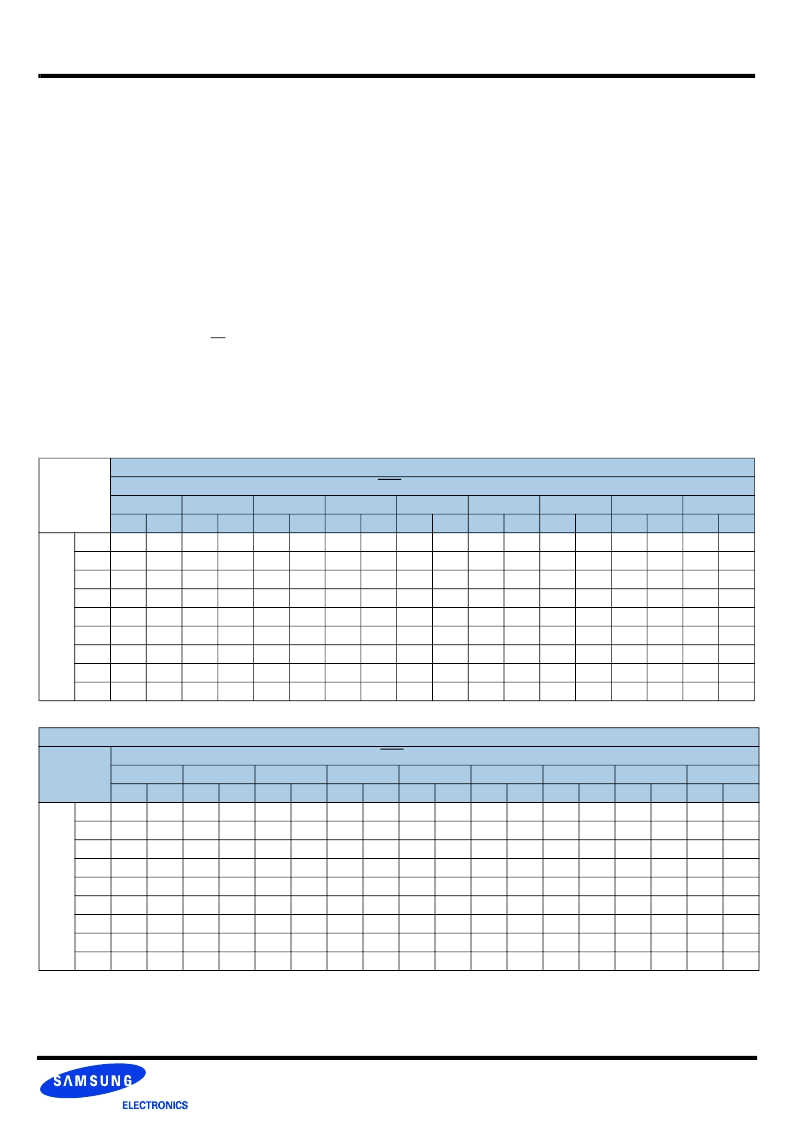
tDS,
tDH Derating Values of gDDR2-550 (ALL units in ‘ps’, Note 1 applies to entire Table)
DQS,DQS Differential Slew Rate
4.0 V/ns
3.0 V/ns
2.0 V/ns
1.8 V/ns
1.6 V/ns
1.4V/ns
1.2V/ns
1.0V/ns
0.8V/ns
tDS
tDH
tDS
tDH
tDS
tDH
tDS
tDH
tDS
tDH
tDS
tDH
tDS
tDH
tDS
tDH
tDS
tDH
DQ
Slew
rate
V/ns
2.0
125
45
125
45
125
45
-
-
-
-
-
-
-
-
-
-
-
-
1.5
83
21
83
21
83
21
95
33
-
-
-
-
-
-
-
-
-
-
1.0
0
0
0
0
0
0
12
12
24
24
-
-
-
-
-
-
-
-
0.9
-
-
-11
-14
-11
-14
1
-2
13
10
25
22
-
-
-
-
-
-
0.8
-
-
-
-
-25
-31
-13
-19
-1
-7
11
5
23
17
-
-
-
-
0.7
-
-
-
-
-
-
-31
-42
-19
-30
-7
-18
5
-6
17
6
-
-
0.6
-
-
-
-
-
-
-
-
-43
-59
-31
-47
-19
-35
-7
-23
5
-11
0.5
-
-
-
-
-
-
-
-
-
-
-74
-89
-62
-77
-50
-65
-38
-53
0.4
-
-
-
-
-
-
-
-
-
-
-
-
-127
-140
-115
-128
-103
-116
tDS,
tDH Derating Values for gDDR2-600/700/800 (ALL units in ‘ps’, Note 1 applies to entire Table)
DQS,DQS Differential Slew Rate
4.0 V/ns
3.0 V/ns
2.0 V/ns
1.8 V/ns
1.6 V/ns
1.4V/ns
1.2V/ns
1.0V/ns
0.8V/ns
tDS
tDH
tDS
tDH
tDS
tDH
tDS
tDH
tDS
tDH
tDS
tDH
tDS
tDH
tDS
tDH
tDS
tDH
DQ
Slew
rate
V/ns
2.0
100
45
100
45
100
45
-
-
-
-
-
-
-
-
-
-
-
-
1.5
67
21
67
21
67
21
79
33
-
-
-
-
-
-
-
-
-
-
1.0
0
0
0
0
0
0
12
12
24
24
-
-
-
-
-
-
-
-
0.9
-
-
-5
-14
-5
-14
7
-2
19
10
31
22
-
-
-
-
-
-
0.8
-
-
-
-
-13
-31
-1
-19
11
-7
23
5
35
17
-
-
-
-
0.7
-
-
-
-
-
-
-10
-42
2
-30
14
-18
26
-6
38
6
-
-
0.6
-
-
-
-
-
-
-
-
-10
-59
2
-47
14
-35
26
-23
38
-11
0.5
-
-
-
-
-
-
-
-
-
-
-24
-89
-12
-77
0
-65
12
-53
0.4
-
-
-
-
-
-
-
-
-
-
-
-
-52
-140
-40
-128
-28
-116
相關(guān)PDF資料 |
PDF描述 |
|---|---|
| K4N51163QC-ZC36 | 512Mbit gDDR2 SDRAM |
| K4R271669B-N(M)CG6 | 256K x 16/18 bit x 32s banks Direct RDRAMTM |
| K4R271669B-N(M)CK7 | 256K x 16/18 bit x 32s banks Direct RDRAMTM |
| K4R271669B-Nb(M)CcK8 | 256K x 16/18 bit x 32s banks Direct RDRAMTM |
| K4R271669B | 256K x 16/18 bit x 32s banks Direct RDRAMTM |
相關(guān)代理商/技術(shù)參數(shù) |
參數(shù)描述 |
|---|---|
| K4N51163QC-ZC36 | 制造商:SAMSUNG 制造商全稱:Samsung semiconductor 功能描述:512Mbit gDDR2 SDRAM |
| K4N51163QG | 制造商:SAMSUNG 制造商全稱:Samsung semiconductor 功能描述:Graphic Memory |
| K4N51163QZ | 制造商:SAMSUNG 制造商全稱:Samsung semiconductor 功能描述:Graphic Memory |
| K4N56163QF | 制造商:SAMSUNG 制造商全稱:Samsung semiconductor 功能描述:256Mbit gDDR2 SDRAM |
| K4N56163QF-GC | 制造商:SAMSUNG 制造商全稱:Samsung semiconductor 功能描述:256Mbit gDDR2 SDRAM |
發(fā)布緊急采購,3分鐘左右您將得到回復(fù)。