- 您現(xiàn)在的位置:買賣IC網(wǎng) > PDF目錄374277 > K4N51163QC-ZC36 (SAMSUNG SEMICONDUCTOR CO. LTD.) 512Mbit gDDR2 SDRAM PDF資料下載
參數(shù)資料
| 型號: | K4N51163QC-ZC36 |
| 廠商: | SAMSUNG SEMICONDUCTOR CO. LTD. |
| 英文描述: | 512Mbit gDDR2 SDRAM |
| 中文描述: | 512MB的GDDR2 SDRAM的 |
| 文件頁數(shù): | 64/64頁 |
| 文件大小: | 1420K |
| 代理商: | K4N51163QC-ZC36 |
第1頁第2頁第3頁第4頁第5頁第6頁第7頁第8頁第9頁第10頁第11頁第12頁第13頁第14頁第15頁第16頁第17頁第18頁第19頁第20頁第21頁第22頁第23頁第24頁第25頁第26頁第27頁第28頁第29頁第30頁第31頁第32頁第33頁第34頁第35頁第36頁第37頁第38頁第39頁第40頁第41頁第42頁第43頁第44頁第45頁第46頁第47頁第48頁第49頁第50頁第51頁第52頁第53頁第54頁第55頁第56頁第57頁第58頁第59頁第60頁第61頁第62頁第63頁當前第64頁
- 64 -
Rev 1.5 Oct. 2005
512M gDDR2 SDRAM
K4N51163QC-ZC
gDDR2 SDRAM Default Output Driver V–I Characteristics
gDDR2 SDRAM output driver characteristics are defined for full strength default operation as selected by the EMRS1 bits A7-A9 = ‘111’.
Figures 1 and 2 show the driver characteristics graphically, and tables 1 and 2 show the same data in tabular format suitable for input
into simulation tools. The driver characteristics evaluation conditions are:
Nominal Default 25
o
C (T case), VDDQ = 1.8 V, typical process
Minimum TBD
o
C (T case), VDDQ = 1.7 V, slow–slow process
Maximum 0
o
C (T case), VDDQ = 1.9 V, fast–fast process
Default Output Driver Characteristic Curves Notes:
1) The full variation in driver current from minimum to maximum process, temperature, and voltage will lie within the outer bounding lines
of the V–I curve of figures 1 and 2.
2) It is recommended that the ”typical” IBIS V–I curve lie within the inner bounding lines of the V–I curves of figures 1 and 2.
Table 3.
Full Strength Calibrated Pulldown Driver Characteristics
Table 4.
Full Strength Calibrated Pullup Driver Characteristics
gDDR2 SDRAM Calibrated Output Driver V–I Characteristics
gDDR2 SDRAM output driver characteristics are defined for full strength calibrated operation as selected by the procedure outlined in
Off-Chip Driver (OCD) Impedance Adjustment. Tables 3 and 4 show the data in tabular format suitable for input into simulation tools. The
nominal points represent a device at exactly 18 ohms. The nominal low and nominal high values represent the range that can be
achieved with a maximum 1.5 ohm step size with no calibration error at the exact nominal conditions only (i.e. perfect calibration proce-
dure, 1.5 ohm maximum step size guaranteed by specification). Real system calibration error needs to be added to these values. It
must be understood that these V-I curves as represented here or in supplier IBIS models need to be adjusted to a wider range as a
result of any system calibration error. Since this is a system specific phenomena, it cannot be quantified here. The values in the cali-
brated tables represent just the DRAM portion of uncertainty while looking at one DQ only. If the calibration procedure is used, it is pos-
sible to cause the device to operate outside the bounds of the default device characteristics tables and figures. In such a situation, the
timing parameters in the specification cannot be guaranteed. It is solely up to the system application to ensure that the device is cali-
brated between the minimum and maximum default values at all times. If this can’t be guaranteed by the system calibration procedure,
re-calibration policy, and uncertainty with DQ to DQ variation, then it is recommended that only the default values be used. The nominal
maximum and minimum values represent the change in impedance from nominal low and high as a result of voltage and temperature
change from the nominal condition to the maximum and minimum conditions. If calibrated at an extreme condition, the amount of varia-
tion could be as much as from the nominal minimum to the nominal maximum or vice versa. The driver characteristics evaluation condi-
tions are:
Nominal 25
o
C (T case), VDDQ = 1.8 V, typical process.
Nominal Low and Nominal High 25
o
C (T case), VDDQ = 1.8 V, any process.
Nominal Minimum TBD
o
C (T case), VDDQ = 1.7 V, any process.
Nominal Maximum 0
o
C (T case), VDDQ = 1.9 V, any process.
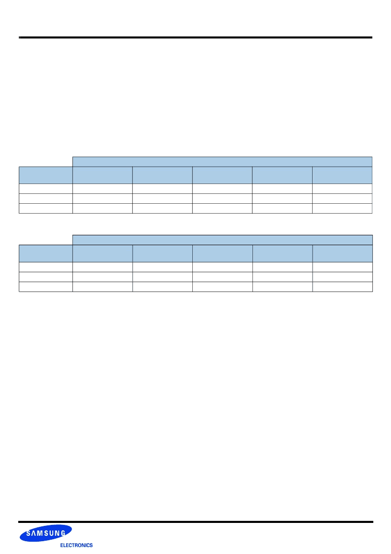
Calibrated Pulldown Current (mA)
Voltage (V)
Nominal Minimum
(21 Ohms)
Nominal Low
(18.75 ohms)
Nominal
(18 ohms)
Nominal High
(17.25 ohms)
Nominal Maximum
(15 Ohms)
0.2
9.5
10.7
11.5
11.8
13.3
0.3
14.3
16.0
16.6
17.4
20.0
0.4
18.7
21.0
21.6
23.0
27.0
Calibrated Pulldown Current (mA)
Voltage (V)
Nominal Minimum
(21 Ohms)
Nominal Low
(18.75 ohms)
Nominal
(18 ohms)
Nominal High
(17.25 ohms)
Nominal Maximum
(15 Ohms)
0.2
-9.5
-10.7
-11.4
-11.8
-13.3
0.3
-14.3
-16.0
-16.5
-17.4
-20.0
0.4
-18.7
-21.0
-21.2
-23.0
-27.0
相關(guān)PDF資料 |
PDF描述 |
|---|---|
| K4R271669B-N(M)CG6 | 256K x 16/18 bit x 32s banks Direct RDRAMTM |
| K4R271669B-N(M)CK7 | 256K x 16/18 bit x 32s banks Direct RDRAMTM |
| K4R271669B-Nb(M)CcK8 | 256K x 16/18 bit x 32s banks Direct RDRAMTM |
| K4R271669B | 256K x 16/18 bit x 32s banks Direct RDRAMTM |
| K4R441869B | 256K x 16/18 bit x 32s banks Direct RDRAMTM |
相關(guān)代理商/技術(shù)參數(shù) |
參數(shù)描述 |
|---|---|
| K4N51163QG | 制造商:SAMSUNG 制造商全稱:Samsung semiconductor 功能描述:Graphic Memory |
| K4N51163QZ | 制造商:SAMSUNG 制造商全稱:Samsung semiconductor 功能描述:Graphic Memory |
| K4N56163QF | 制造商:SAMSUNG 制造商全稱:Samsung semiconductor 功能描述:256Mbit gDDR2 SDRAM |
| K4N56163QF-GC | 制造商:SAMSUNG 制造商全稱:Samsung semiconductor 功能描述:256Mbit gDDR2 SDRAM |
| K4N56163QF-GC25 | 制造商:SAMSUNG 制造商全稱:Samsung semiconductor 功能描述:256Mbit gDDR2 SDRAM |
發(fā)布緊急采購,3分鐘左右您將得到回復(fù)。