- 您現(xiàn)在的位置:買賣IC網(wǎng) > PDF目錄374277 > K4N51163QC-ZC (SAMSUNG SEMICONDUCTOR CO. LTD.) 512Mbit gDDR2 SDRAM PDF資料下載
參數(shù)資料
| 型號(hào): | K4N51163QC-ZC |
| 廠商: | SAMSUNG SEMICONDUCTOR CO. LTD. |
| 英文描述: | 512Mbit gDDR2 SDRAM |
| 中文描述: | 512MB的GDDR2 SDRAM的 |
| 文件頁數(shù): | 36/64頁 |
| 文件大小: | 1420K |
| 代理商: | K4N51163QC-ZC |
第1頁第2頁第3頁第4頁第5頁第6頁第7頁第8頁第9頁第10頁第11頁第12頁第13頁第14頁第15頁第16頁第17頁第18頁第19頁第20頁第21頁第22頁第23頁第24頁第25頁第26頁第27頁第28頁第29頁第30頁第31頁第32頁第33頁第34頁第35頁當(dāng)前第36頁第37頁第38頁第39頁第40頁第41頁第42頁第43頁第44頁第45頁第46頁第47頁第48頁第49頁第50頁第51頁第52頁第53頁第54頁第55頁第56頁第57頁第58頁第59頁第60頁第61頁第62頁第63頁第64頁
- 36 -
Rev 1.5 Oct. 2005
512M gDDR2 SDRAM
K4N51163QC-ZC
CMD
NOP
NOP
NOP
NOP
NOP
NOP
NOP
DQs
NOP
CK/CK
DOUTA
0
DOUTA
1
DOUTA
2
DOUTA
3
READ A
Posted CAS
AL = 2
CL =3
RL = 5
DQS
=< t
DQSCK
T0
T2
T1
T3
T4
T5
T6
T7
T8
t
CH
t
CL
CK
CK
CK
DQS
DQ
DQS
DQS
t
RPST
Q
t
RPRE
t
DQSQmax
t
QH
t
QH
t
DQSQmax
Q
Q
Q
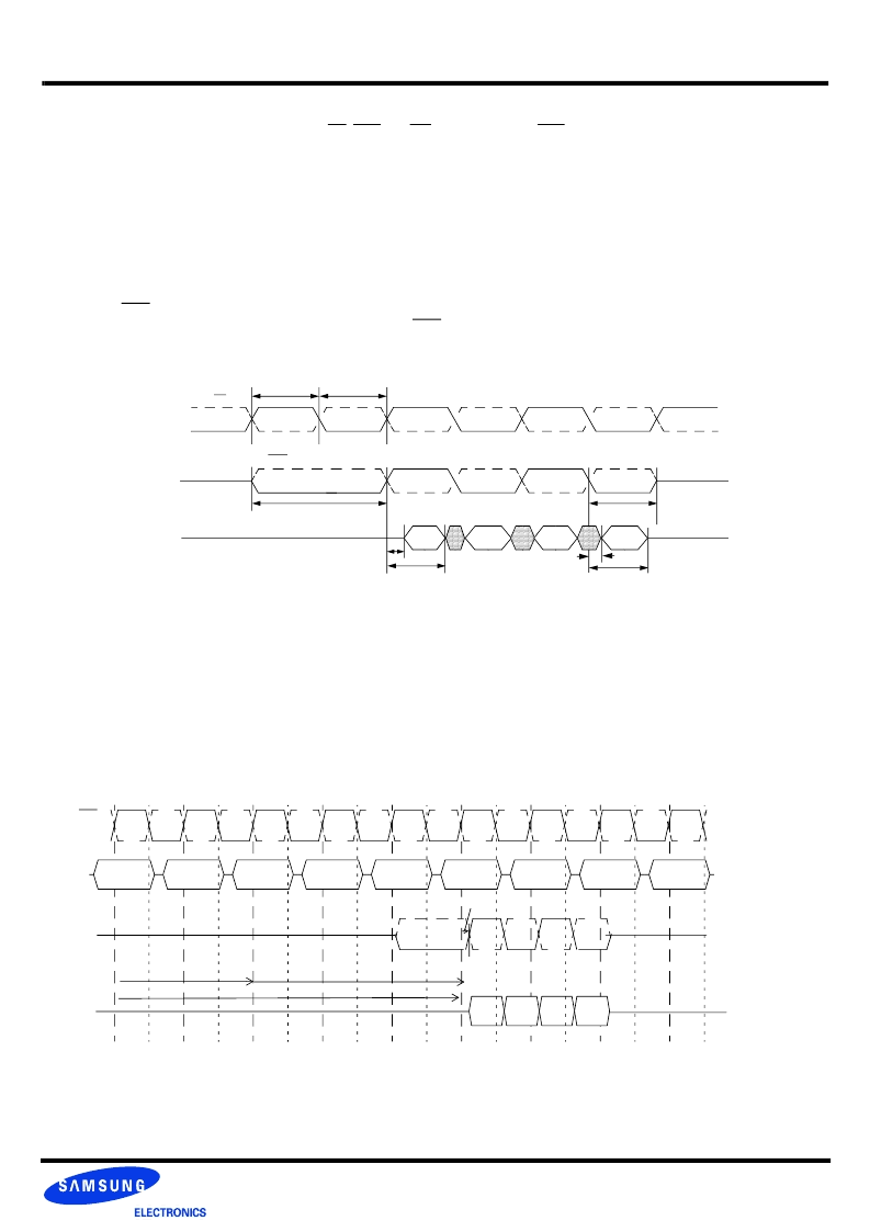
Burst Read Operation: RL = 5 (AL = 2, CL = 3, BL = 4)
The Burst Write command is initiated by having CS, CAS and WE low while holding RAS high at the rising edge of the clock. The
address inputs determine the starting column address. Write latency (WL) is defined by a read latency (RL) minus one and is equal to
(AL + CL -1). A data strobe signal (DQS) should be driven low (preamble) one clock prior to the WL. The first data bit of the burst cycle
must be applied to the DQ pins at the first rising edge of the DQS following the preamble. The tDQSS specification must be satisfied for
write cycles. The subsequent burst bit data are issued on successive edges of the DQS until the burst length is completed, which is 4 or
8 bit burst. When the burst has finished, any additional data supplied to the DQ pins will be ignored. The DQ Signal is ignored after the
burst write operation is complete. The time from the completion of the burst write to bank precharge is the write recovery time (WR).
gDDR2 SDRAM pin timings are specified for either single ended mode or differen-tial mode depending on the setting of the EMRS
“Enable DQS” mode bit; timing advantages of differential mode are realized in system design. The method by which the gDDR2 SDRAM
pin timings are measured is mode dependent. In single ended mode, timing relationships are measured relative to the rising or falling
edges of DQS crossing at V
REF
. In differential mode, these timing relationships are measured relative to the crosspoint of DQS and its
complement, DQS. This distinction in timing methods is guaranteed by design and characterization. Note that when differential data
strobe mode is disabled via the EMRS, the complementary pin, DQS, must be tied externally to VSS through a 20 ohm to 10K ohm
resistor to insure proper operation.
Burst Read Command
相關(guān)PDF資料 |
PDF描述 |
|---|---|
| K4N51163QC-ZC25 | ; Filter Type:RFI; Current Rating:180A; Voltage Rating:480V; Series:FN258 RoHS Compliant: Yes |
| K4N51163QC-ZC2A | 512Mbit gDDR2 SDRAM |
| K4N51163QC-ZC33 | 512Mbit gDDR2 SDRAM |
| K4N51163QC-ZC36 | 512Mbit gDDR2 SDRAM |
| K4R271669B-N(M)CG6 | 256K x 16/18 bit x 32s banks Direct RDRAMTM |
相關(guān)代理商/技術(shù)參數(shù) |
參數(shù)描述 |
|---|---|
| K4N51163QC-ZC25 | 制造商:SAMSUNG 制造商全稱:Samsung semiconductor 功能描述:512Mbit gDDR2 SDRAM |
| K4N51163QC-ZC2A | 制造商:SAMSUNG 制造商全稱:Samsung semiconductor 功能描述:512Mbit gDDR2 SDRAM |
| K4N51163QC-ZC33 | 制造商:SAMSUNG 制造商全稱:Samsung semiconductor 功能描述:512Mbit gDDR2 SDRAM |
| K4N51163QC-ZC36 | 制造商:SAMSUNG 制造商全稱:Samsung semiconductor 功能描述:512Mbit gDDR2 SDRAM |
| K4N51163QG | 制造商:SAMSUNG 制造商全稱:Samsung semiconductor 功能描述:Graphic Memory |
發(fā)布緊急采購,3分鐘左右您將得到回復(fù)。