- 您現(xiàn)在的位置:買賣IC網(wǎng) > PDF目錄374277 > K4R761869A-F (SAMSUNG SEMICONDUCTOR CO. LTD.) 576Mbit RDRAM (A-die) 1M x 18bit x 32s banks Direct RDRAMTM PDF資料下載
參數(shù)資料
| 型號: | K4R761869A-F |
| 廠商: | SAMSUNG SEMICONDUCTOR CO. LTD. |
| 英文描述: | 576Mbit RDRAM (A-die) 1M x 18bit x 32s banks Direct RDRAMTM |
| 中文描述: | 576Mbit的RDRAM(一模)100萬x 18位x 32秒銀行直接RDRAMTM |
| 文件頁數(shù): | 18/20頁 |
| 文件大?。?/td> | 313K |
| 代理商: | K4R761869A-F |
Direct RDRAM
Page 16
Version 1.41 Jan. 2004
K4R761869A
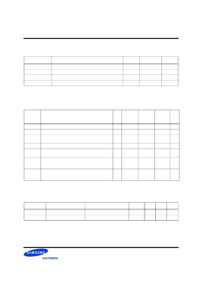
Absolute Maximum Ratings
Note*) Component : refer to T
J,
Θ
JC
Module : refre to T
PLATE, MAX
I
DD
- Supply Current Profile
Table 14: Absolute Maximum Ratings
Symbol
Parameter
Min
Max
Unit
V
I,ABS
Voltage applied to any RSL or CMOS pin with respect to Gnd
- 0.3
V
DD
+0.3
V
V
DD,ABS
, V
DDA,ABS
Voltage on VDD and VDDA with respect to Gnd
- 0.5
V
DD
+1.0
V
T
STORE
Storage temperature
- 50
100
°
C
T
MIN
Minimum operation temperature
0
Note*
°
C
Table 15: Supply Current Profile
I
DD
value
RDRAM Power State and Steady-State Transaction Rates
a
Min
Max
(1200MHz
, -32)
Max
(1066MHz
, -32P)
Max
(800MHz,
-40)
Unit
I
DD,PDN
Device in PDN, self-refresh enabled and INIT.LSR=0.
-
9000
9000
9000
μ
A
I
DD,NAP
Device in NAP.
-
4
4
4
mA
I
DD,STBY
Device in STBY. This is the average for a device in STBY with (1) no
packets on the Channel, and (2) with packets sent to other devices.
-
110
110
95
mA
I
DD,REFRESH
Device in STBY and refreshing rows at the t
REF,MAX
period.
-
110
110
95
mA
I
DD,ATTN
Device in ATTN. This is the average for a device in ATTN with (1) no
packets on the Channel, and (2) with packets sent to other devices.
-
165
160
135
mA
I
DD,ATTN-W
Device in ATTN. ACT command every 8t
CYCLE
, PRE command
every 8t
CYCLE
, WR command every 4
t
CYCLE
, and data is
1100..1100
-
980(x18)
b
930(x18)
730(x18)
mA
I
DD,ATTN-R
Device in ATTN. ACT command every 8t
CYCLE
, PRE command
every 8
t
Cc
, RD command every 4
t
CYCLE
, and data is
1111..1111
-
960(x18)
900(x18)
720(x18)
mA
a. CMOS interface consumes power in all power states.
b. x18 RDRAM device data width.
c. This does not include the I
OL
sink current. The RDRAM device dissipates I
OL
V
OL
in each output driver when a logic one is driven.
Table 16: Supply Current at Initialization
Symbol
Parameter
Allowed Range of t
CYCLE
V
DD
Min
Max
Unit
I
DD,PWRUP,D
I
DD
from power -on to SETR
1.667ns to 2.5ns
V
DD,MIN
-
200
a
mA
I
DD,SETR,D
I
DD
from SETR to CLRR
1.667ns to 2.5ns
V
DD,MIN
-
332
mA
a. The supply current will be 150mA when tCYCLE is in the range 15ns to 1000ns.
相關(guān)PDF資料 |
PDF描述 |
|---|---|
| K4R761869A-FbCcN1 | 576Mbit RDRAM (A-die) 1M x 18bit x 32s banks Direct RDRAMTM |
| K4R761869A-FCM8 | 576Mbit RDRAM (A-die) 1M x 18bit x 32s banks Direct RDRAMTM |
| K4R761869A-FCT9 | 576Mbit RDRAM (A-die) 1M x 18bit x 32s banks Direct RDRAMTM |
| K4R761869A-GCM8 | 576Mbit RDRAM (A-die) 1M x 18bit x 32s banks Direct RDRAMTM |
| K4R881869 | 288Mbit RDRAM 512K x 18 bit x 2*16 Dependent Banks Direct RDRAMTM |
相關(guān)代理商/技術(shù)參數(shù) |
參數(shù)描述 |
|---|---|
| K4R761869A-FBCCN1 | 制造商:SAMSUNG 制造商全稱:Samsung semiconductor 功能描述:576Mbit RDRAM (A-die) 1M x 18bit x 32s banks Direct RDRAMTM |
| K4R761869A-FCM8 | 制造商:SAMSUNG 制造商全稱:Samsung semiconductor 功能描述:576Mbit RDRAM (A-die) 1M x 18bit x 32s banks Direct RDRAMTM |
| K4R761869A-FCT9 | 制造商:SAMSUNG 制造商全稱:Samsung semiconductor 功能描述:576Mbit RDRAM (A-die) 1M x 18bit x 32s banks Direct RDRAMTM |
| K4R761869A-GCM8 | 制造商:SAMSUNG 制造商全稱:Samsung semiconductor 功能描述:576Mbit RDRAM (A-die) 1M x 18bit x 32s banks Direct RDRAMTM |
| K4R761869A-GCN1 | 制造商:SAMSUNG 制造商全稱:Samsung semiconductor 功能描述:576Mbit RDRAM (A-die) 1M x 18bit x 32s banks Direct RDRAMTM |
發(fā)布緊急采購,3分鐘左右您將得到回復(fù)。