- 您現(xiàn)在的位置:買賣IC網(wǎng) > PDF目錄374277 > K4R761869A-FCT9 (SAMSUNG SEMICONDUCTOR CO. LTD.) 576Mbit RDRAM (A-die) 1M x 18bit x 32s banks Direct RDRAMTM PDF資料下載
參數(shù)資料
| 型號(hào): | K4R761869A-FCT9 |
| 廠商: | SAMSUNG SEMICONDUCTOR CO. LTD. |
| 英文描述: | 576Mbit RDRAM (A-die) 1M x 18bit x 32s banks Direct RDRAMTM |
| 中文描述: | 576Mbit的RDRAM(一模)100萬x 18位x 32秒銀行直接RDRAMTM |
| 文件頁數(shù): | 17/20頁 |
| 文件大小: | 313K |
| 代理商: | K4R761869A-FCT9 |
Direct RDRAM
Page 15
K4R761869A
Version 1.41 Jan. 2004
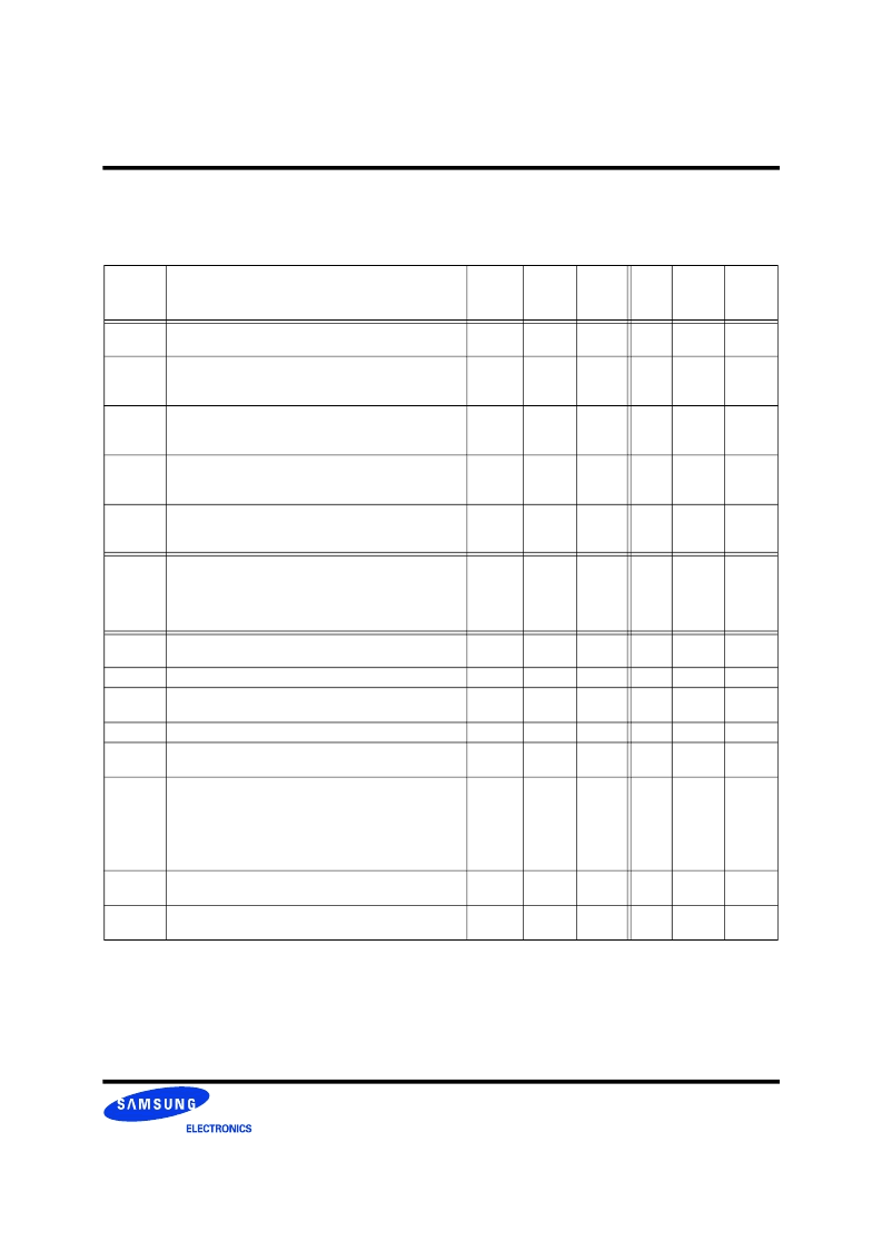
Timing Parameters
Table 13: Timing Parameter Summary
Parameter
Description
Min
-32
-1200
Min
-32P
-1066
Min
-40
-800
Max
Units
Figure(s)
t
RC
Row Cycle time of RDRAM banks -the interval between ROWA
packets with ACT commands to the same bank.
32
28
28
-
t
CYCLE
Figure 16
Figure 17
t
RAS
RAS-asserted time of RDRAM bank - the interval between ROWA
packet with ACT command and next ROWR packet with PRER
a
command to the same bank.
22
20
20
64
μ
s
b
t
CYCLE
Figure 16
Figure 17
t
RP
Row Precharge time of RDRAM banks - the interval between ROWR
packet with PRER
a
command and next ROWA packet with ACT
command to the same bank.
10
8
8
-
t
CYCLE
Figure 16
Figure 17
t
PP
Precharge-to-precharge time of RDRAM device - the interval
between successive ROWR packets with PRER
a
commands to any
banks of the same device.
8
8
8
-
t
CYCLE
Figure 13
t
RR
RAS-to-RAS time of RDRAM device - the interval between succes-
sive ROWA packets with ACT commands to any banks of the same
device.
8
8
8
-
t
CYCLE
Figure 14
t
RCD
RAS-to-CAS Delay - the interval from ROWA packet with ACT
command to COLC packet with RD or WR command). Note - the
RAS-to-CAS delay seen by the RDRAM core (t
RCD-C
) is equal to
t
RCD-C
= 1 + t
RCD
because of differences in the row and column paths
through the RDRAM interface.
9
9
7
-
t
CYCLE
Figure 16
Figure 17
t
CAC
CAS Access delay - the interval from RD command to Q read data.
The equation for t
CAC
is given in the TPARM register in Figure 40.
9
8
8
12
t
CYCLE
Figure 5
Figure 40
t
CWD
CAS Write Delay (interval from WR command to D write data.
6
6
6
6
t
CYCLE
Figure 5
t
CC
CAS-to-CAS time of RDRAM bank - the interval between successive
COLC commands).
4
4
4
-
t
CYCLE
Figure 16
Figure 17
t
PACKET
Length of ROWA, ROWR, COLC, COLM or COLX packet.
4
4
4
4
t
CYCLE
Figure 3
t
RTR
Interval from COLC packet with WR command to COLC packet
which causes retire, and to COLM packet with bytemask.
8
8
8
-
t
CYCLE
Figure 18
t
OFFP
The interval (offset) from COLC packet with RDA command, or
from COLC packet with retire command (after WRA automatic pre-
charge), or from COLC packet with PREC command, or from COLX
packet with PREX command to the equivalent ROWR packet with
PRER. The equation for t
OFFP
is given in the TPARM register in
Figure 40.
4
4
4
4
t
CYCLE
Figure 15
Figure 40
t
RDP
Interval from last COLC packet with RD command to ROWR packet
with PRER.
4
4
4
-
t
CYCLE
Figure 16
t
RTP
Interval from last COLC packet with automatic retire command to
ROWR packet with PRER.
4
4
4
-
t
CYCLE
Figure 17
a. Or equivalent PREC or PREX command. See Figure 15.
b. This is a constraint imposed by the core, and is therefore in units of
μ
s rather than t
CYCLE
.
相關(guān)PDF資料 |
PDF描述 |
|---|---|
| K4R761869A-GCM8 | 576Mbit RDRAM (A-die) 1M x 18bit x 32s banks Direct RDRAMTM |
| K4R881869 | 288Mbit RDRAM 512K x 18 bit x 2*16 Dependent Banks Direct RDRAMTM |
| K4R881869M | 288Mbit RDRAM 512K x 18 bit x 2*16 Dependent Banks Direct RDRAMTM |
| K4R881869M-NbCcG6 | 288Mbit RDRAM 512K x 18 bit x 2*16 Dependent Banks Direct RDRAMTM |
| K4R881869M-NCK7 | 288Mbit RDRAM 512K x 18 bit x 2*16 Dependent Banks Direct RDRAMTM |
相關(guān)代理商/技術(shù)參數(shù) |
參數(shù)描述 |
|---|---|
| K4R761869A-GCM8 | 制造商:SAMSUNG 制造商全稱:Samsung semiconductor 功能描述:576Mbit RDRAM (A-die) 1M x 18bit x 32s banks Direct RDRAMTM |
| K4R761869A-GCN1 | 制造商:SAMSUNG 制造商全稱:Samsung semiconductor 功能描述:576Mbit RDRAM (A-die) 1M x 18bit x 32s banks Direct RDRAMTM |
| K4R761869A-GCT9 | 制造商:SAMSUNG 制造商全稱:Samsung semiconductor 功能描述:576Mbit RDRAM (A-die) 1M x 18bit x 32s banks Direct RDRAMTM |
| K4R761869A-GCT9000 | 制造商:Samsung Semiconductor 功能描述:512 DIRECT RDRAM X18 WBGA - Trays |
| K4R881869 | 制造商:SAMSUNG 制造商全稱:Samsung semiconductor 功能描述:288Mbit RDRAM 512K x 18 bit x 2*16 Dependent Banks Direct RDRAMTM |
發(fā)布緊急采購,3分鐘左右您將得到回復(fù)。