- 您現(xiàn)在的位置:買賣IC網(wǎng) > PDF目錄374277 > K4R761869A-GCN1 (SAMSUNG SEMICONDUCTOR CO. LTD.) 576Mbit RDRAM (A-die) 1M x 18bit x 32s banks Direct RDRAMTM PDF資料下載
參數(shù)資料
| 型號(hào): | K4R761869A-GCN1 |
| 廠商: | SAMSUNG SEMICONDUCTOR CO. LTD. |
| 英文描述: | 576Mbit RDRAM (A-die) 1M x 18bit x 32s banks Direct RDRAMTM |
| 中文描述: | 576Mbit的RDRAM(一模)100萬x 18位x 32秒銀行直接RDRAMTM |
| 文件頁(yè)數(shù): | 14/20頁(yè) |
| 文件大?。?/td> | 313K |
| 代理商: | K4R761869A-GCN1 |
第1頁(yè)第2頁(yè)第3頁(yè)第4頁(yè)第5頁(yè)第6頁(yè)第7頁(yè)第8頁(yè)第9頁(yè)第10頁(yè)第11頁(yè)第12頁(yè)第13頁(yè)當(dāng)前第14頁(yè)第15頁(yè)第16頁(yè)第17頁(yè)第18頁(yè)第19頁(yè)第20頁(yè)
Direct RDRAM
Page 12
Version 1.41 Jan. 2004
K4R761869A
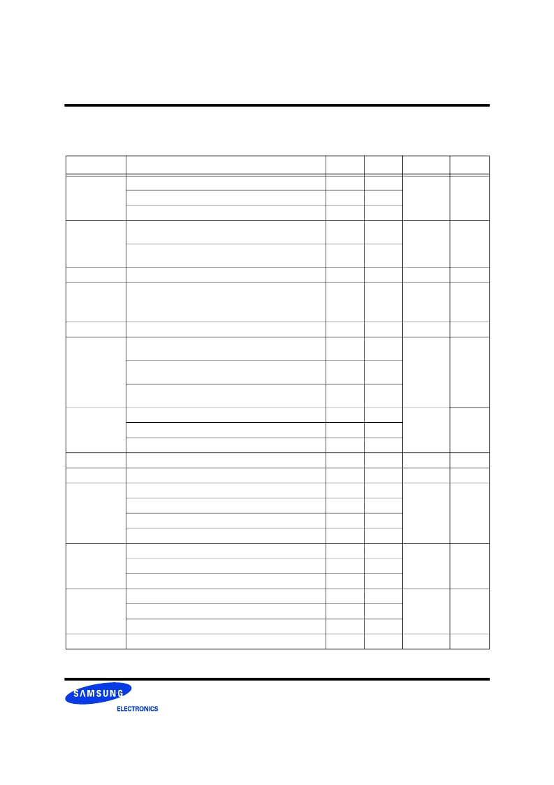
Timing Conditions
Table 11: Timing Conditions
Symbol
Parameter
Min
Max
Unit
Figure(s)
t
CYCLE
CTM and CFM cycle times (-1200)
1.667
2.5
ns
Figure 56
CTM and CFM cycle times (-1066)
1.875
2.5
CTM and CFM cycle times (-800)
2.50
3.33
t
CR
, t
CF
CTM and CFM input rise and fall times. Use the minimum value of
these parameters during testing. (-1200)
0.2
0.45
ns
Figure 56
CTM and CFM input rise and fall times. Use the minimum value of
these parameters during testing. (-1066,-800)
0.2
0.5
t
CH
, t
CL
CTM and CFM high and low times
40%
60%
t
CYCLE
Figure 56
t
TR
CTM-CFM differential (MSE/MS=0/0)
CTM-CFM differential (MSE/MS=1/1)
a
CTM-CFM differential only for 1.875ns and 1.667ns (MSE/MS=1/0)
0.0
0.9
-0.1
1.0
1.0
0.1
t
CYCLE
Figure 43
Figure 56
t
DCW
Domain crossing window
-0.1
0.1
t
CYCLE
Figure 62
t
DR
, t
DF
DQA/DQB/ROW/COL input rise/fall times (20% to 80%). Use the
minimum value of these parameters during testing.@ t
CYCLE
=1.667ns
0.2
0.45
ns
Figure 57
DQA/DQB/ROW/COL input rise/fall times (20% to 80%). Use the
minimum value of these parameters during testing.@ t
CYCLE
=1.875ns
0.2
0.45
DQA/DQB/ROW/COL input rise/fall times (20% to 80%). Use the
minimum value of these parameters during testing.@ t
CYCLE
=2.50ns
0.2
0.65
t
S
, t
H
DQA/DQB/ROW/COL-to-CFM set/hold @ t
CYCLE
=1.667ns
0.140
b
-
ns
Figure 57
DQA/DQB/ROW/COL-to-CFM set/hold @ t
CYCLE
=1.875ns
0.160
b,c
-
DQA/DQB/ROW/COL-to-CFM set/hold @ t
CYCLE
=2.50ns
0.200
b.d
-
t
DR1,
t
DF1
SIO0, SIO1 input rise and fall times
-
5.0
ns
Figure 59
t
DR2,
t
DF2
CMD, SCK input rise and fall times
-
2.0
ns
Figure 59
t
CYCLE1
SCK cycle time - Serial control register transactions
1000
-
ns
Figure 59
SCK cycle time - Power transitions @ t
CYCLE
=1.667ns
7.5
-
SCK cycle time - Power transitions @ t
CYCLE
=1.875ns
7.5
-
SCK cycle time - Power transitions @ t
CYCLE
=2.50ns
10
-
t
CH1
, t
CL1
SCK high and low times @ t
CYCLE
=1.667ns
3.5
-
ns
Figure 59
SCK high and low times @ t
CYCLE
=1.875ns
3.5
-
SCK high and low times @ t
CYCLE
=2.50ns
4.25
-
t
S1
CMD setup time to SCK rising or falling edge
e
@ t
CYCLE
=1.667ns
1.0
-
ns
Figure 59
CMD setup time to SCK rising or falling edge
e
@ t
CYCLE
=1.875ns
1.0
-
CMD setup time to SCK rising or falling edge
e
@ t
CYCLE
=2.50ns
1.25
-
t
H1
CMD hold time to SCK rising or falling edge
e
1
-
ns
Figure 59
相關(guān)PDF資料 |
PDF描述 |
|---|---|
| K4R761869A-GCT9 | 576Mbit RDRAM (A-die) 1M x 18bit x 32s banks Direct RDRAMTM |
| K4R761869A-F | 576Mbit RDRAM (A-die) 1M x 18bit x 32s banks Direct RDRAMTM |
| K4R761869A-FbCcN1 | 576Mbit RDRAM (A-die) 1M x 18bit x 32s banks Direct RDRAMTM |
| K4R761869A-FCM8 | 576Mbit RDRAM (A-die) 1M x 18bit x 32s banks Direct RDRAMTM |
| K4R761869A-FCT9 | 576Mbit RDRAM (A-die) 1M x 18bit x 32s banks Direct RDRAMTM |
相關(guān)代理商/技術(shù)參數(shù) |
參數(shù)描述 |
|---|---|
| K4R761869A-GCT9 | 制造商:SAMSUNG 制造商全稱:Samsung semiconductor 功能描述:576Mbit RDRAM (A-die) 1M x 18bit x 32s banks Direct RDRAMTM |
| K4R761869A-GCT9000 | 制造商:Samsung Semiconductor 功能描述:512 DIRECT RDRAM X18 WBGA - Trays |
| K4R881869 | 制造商:SAMSUNG 制造商全稱:Samsung semiconductor 功能描述:288Mbit RDRAM 512K x 18 bit x 2*16 Dependent Banks Direct RDRAMTM |
| K4R881869D | 制造商:SAMSUNG 制造商全稱:Samsung semiconductor 功能描述:256/288Mbit RDRAM(D-die) |
| K4R881869D-FCM8 | 制造商:Samsung Electro-Mechanics 功能描述:16M X 18 DIRECT RAMBUS DRAM, PBGA92 |
發(fā)布緊急采購(gòu),3分鐘左右您將得到回復(fù)。