- 您現(xiàn)在的位置:買賣IC網(wǎng) > PDF目錄374277 > K4R881869M-NbCcG6 (SAMSUNG SEMICONDUCTOR CO. LTD.) 288Mbit RDRAM 512K x 18 bit x 2*16 Dependent Banks Direct RDRAMTM PDF資料下載
參數(shù)資料
| 型號(hào): | K4R881869M-NbCcG6 |
| 廠商: | SAMSUNG SEMICONDUCTOR CO. LTD. |
| 英文描述: | 288Mbit RDRAM 512K x 18 bit x 2*16 Dependent Banks Direct RDRAMTM |
| 中文描述: | 288Mbit RDRAM的為512k × 18位× 2 * 16屬銀行直接RDRAMTM |
| 文件頁數(shù): | 18/64頁 |
| 文件大小: | 4084K |
| 代理商: | K4R881869M-NBCCG6 |
第1頁第2頁第3頁第4頁第5頁第6頁第7頁第8頁第9頁第10頁第11頁第12頁第13頁第14頁第15頁第16頁第17頁當(dāng)前第18頁第19頁第20頁第21頁第22頁第23頁第24頁第25頁第26頁第27頁第28頁第29頁第30頁第31頁第32頁第33頁第34頁第35頁第36頁第37頁第38頁第39頁第40頁第41頁第42頁第43頁第44頁第45頁第46頁第47頁第48頁第49頁第50頁第51頁第52頁第53頁第54頁第55頁第56頁第57頁第58頁第59頁第60頁第61頁第62頁第63頁第64頁
Page 16
Direct RDRAM
K4R881869M
Rev. 0.9 Jan. 2000
Preliminary
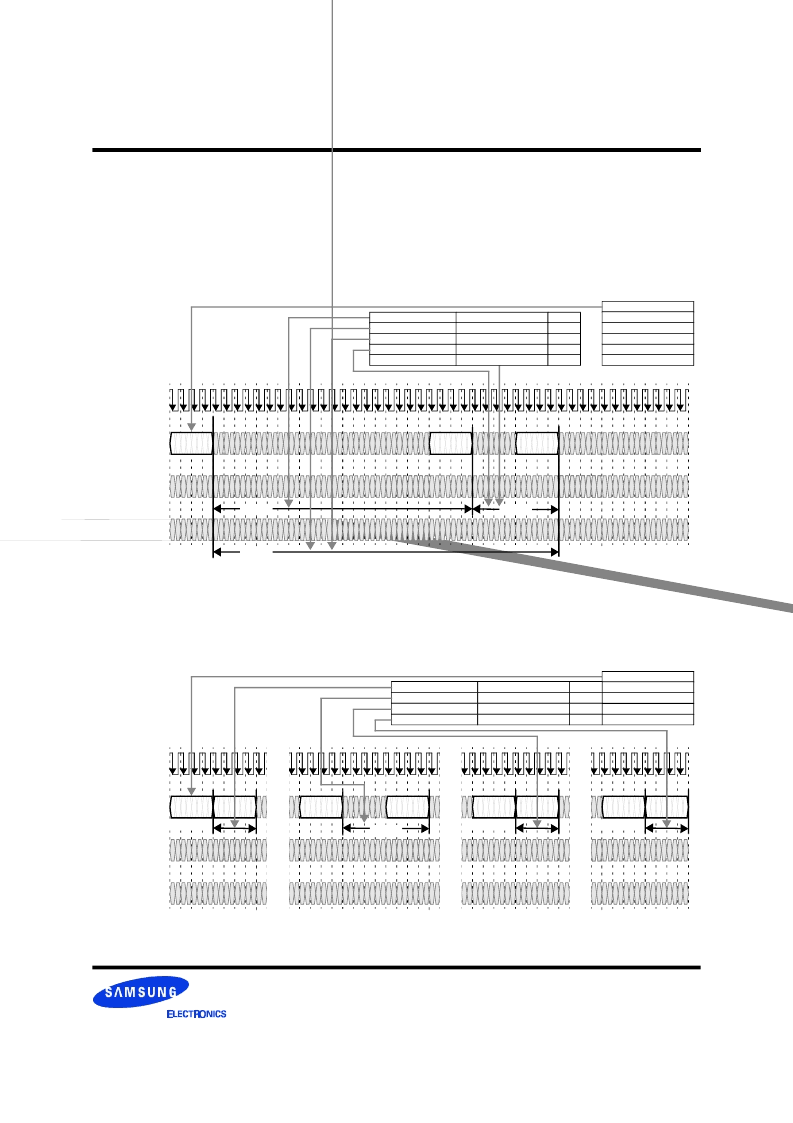
ROW-to-ROW Examples
Figure 10 shows examples of some of the the ROW-to-
ROW packet spacings from Table 10. A complete sequence
of activate and precharge commands is directed to a bank.
The RR8 and RR12 rules apply to this sequence. In addition
to satisfying the t
RAS
and t
RP
timing parameters, the separa-
tion between ACT commands to the same bank must also
satisfy the t
RC
timing parameter (RR4).
When a bank is activated, it is necessary for adjacent banks
to remain precharged. As a result, the adjacent banks will
also satisfy parallel timing constraints; in the example, the
RR11 and RR3 rules are analogous to the RR12 and RR4
rules.
Figure 11 shows examples of the ACT-to-ACT (RR1, RR2)
and ACT-to-PRER (RR5, RR6) command spacings from
Table 10. In general, the commands in ROW packets may be
spaced an interval t
PACKET
apart unless they are directed to
the same or adjacent banks or unless they are a similar
command type (both PRER or both ACT) directed to the
same device.
Figure 10: Row Packet Example
CTM/CFM
DQA8..0
DQB8..0
COL4
..COL0
ROW2
..ROW0
T
0
T
4
T
8
T
12
T
1
T
5
T
9
T
13
T
2
T
6
T
10
T
14
T
3
T
7
T
11
T
15
T
16
T
20
T
24
T
28
T
17
T
21
T
25
T
29
T
18
T
22
T
26
T
30
T
19
T
23
T
27
T
31
T
32
T
36
T
40
T
44
T
33
T
37
T
41
T
45
T
34
T
38
T
42
T
46
T
35
T
39
T
43
T
47
ACT a0
PRER a1
t
RAS
t
RC
a0 = {Da,Ba,Ra}
a1 = {Da,Ba+1}
b0 = {Da,Ba+1,Rb}
b0 = {Da,Ba,Rb}
b0 = {Da,Ba+1,Rb}
b0 = {Da,Ba,Rb}
Same Device
Same Device
Same Device
Adjacent Bank
Adjacent Bank
Same Bank
RR7
RR3
RR4
t
RP
Same Device
Same Device
Adjacent Bank
Same Bank
RR11
RR12
ACT b0
Figure 11: Row Packet Example
CTM/CFM
DQA8..0
DQB8..0
COL4
..COL0
ROW2
..ROW0
T
0
T
4
T
8
T
12
T
1
T
5
T
9
T
13
T
2
T
6
T
10
T
14
T
3
T
7
T
11
T
15
T
16
T
20
T
24
T
28
T
17
T
21
T
25
T
29
T
18
T
22
T
26
T
30
T
19
T
23
T
27
T
31
T
32
T
36
T
40
T
44
T
33
T
37
T
41
T
45
T
34
T
38
T
42
T
46
T
35
T
39
T
43
T
47
ACT a0
PRER b0
t
PACKET
ACT c0
t
RR
a0 = {Da,Ba,Ra}
b0 = {Db,Bb,Rb}
c0 = {Da,Bc,Rc}
b0 = {Db,Bb,Rb}
c0 = {Da,Bc,Rc}
Different Device
Same Device
Different Device
Same Device
Any Bank
Non-adjacent Bank
Any Bank
Non-adjacent Bank
RR1
RR2
RR5
RR6
ACT a0
ACT a0
ACT b0
PRER c0
ACT a0
t
PACKET
t
PACKET
相關(guān)PDF資料 |
PDF描述 |
|---|---|
| K4R881869M-NCK7 | 288Mbit RDRAM 512K x 18 bit x 2*16 Dependent Banks Direct RDRAMTM |
| K4R881869M-NCK8 | 288Mbit RDRAM 512K x 18 bit x 2*16 Dependent Banks Direct RDRAMTM |
| K4S280432A | 128Mbit SDRAM 8M x 4Bit x 4 Banks Synchronous DRAM LVTTL |
| K4S280432C | 128Mbit SDRAM 8M x 4Bit x 4 Banks Synchronous DRAM LVTTL |
| K4S280432F-UC | 128Mb F-die SDRAM Specification 54 TSOP-II with Pb-Free (RoHS compliant) |
相關(guān)代理商/技術(shù)參數(shù) |
參數(shù)描述 |
|---|---|
| K4R881869M-NCK7 | 制造商:SAMSUNG 制造商全稱:Samsung semiconductor 功能描述:288Mbit RDRAM 512K x 18 bit x 2*16 Dependent Banks Direct RDRAMTM |
| K4R881869M-NCK8 | 制造商:SAMSUNG 制造商全稱:Samsung semiconductor 功能描述:288Mbit RDRAM 512K x 18 bit x 2*16 Dependent Banks Direct RDRAMTM |
| K4R881869M-NCK8000 | 制造商:Samsung SDI 功能描述: |
| K4S160822D | 制造商:SAMSUNG 制造商全稱:Samsung semiconductor 功能描述:2Mx8 SDRAM 1M x 8bit x 2 Banks Synchronous DRAM LVTTL |
| K4S160822DT-G/F10 | 制造商:SAMSUNG 制造商全稱:Samsung semiconductor 功能描述:2Mx8 SDRAM 1M x 8bit x 2 Banks Synchronous DRAM LVTTL |
發(fā)布緊急采購,3分鐘左右您將得到回復(fù)。