- 您現(xiàn)在的位置:買賣IC網(wǎng) > PDF目錄374277 > K4R881869M-NbCcG6 (SAMSUNG SEMICONDUCTOR CO. LTD.) 288Mbit RDRAM 512K x 18 bit x 2*16 Dependent Banks Direct RDRAMTM PDF資料下載
參數(shù)資料
| 型號(hào): | K4R881869M-NbCcG6 |
| 廠商: | SAMSUNG SEMICONDUCTOR CO. LTD. |
| 英文描述: | 288Mbit RDRAM 512K x 18 bit x 2*16 Dependent Banks Direct RDRAMTM |
| 中文描述: | 288Mbit RDRAM的為512k × 18位× 2 * 16屬銀行直接RDRAMTM |
| 文件頁數(shù): | 33/64頁 |
| 文件大?。?/td> | 4084K |
| 代理商: | K4R881869M-NBCCG6 |
第1頁第2頁第3頁第4頁第5頁第6頁第7頁第8頁第9頁第10頁第11頁第12頁第13頁第14頁第15頁第16頁第17頁第18頁第19頁第20頁第21頁第22頁第23頁第24頁第25頁第26頁第27頁第28頁第29頁第30頁第31頁第32頁當(dāng)前第33頁第34頁第35頁第36頁第37頁第38頁第39頁第40頁第41頁第42頁第43頁第44頁第45頁第46頁第47頁第48頁第49頁第50頁第51頁第52頁第53頁第54頁第55頁第56頁第57頁第58頁第59頁第60頁第61頁第62頁第63頁第64頁
Page 31
Direct RDRAM
K4R881869M
Rev. 0.9 Jan. 2000
Preliminary
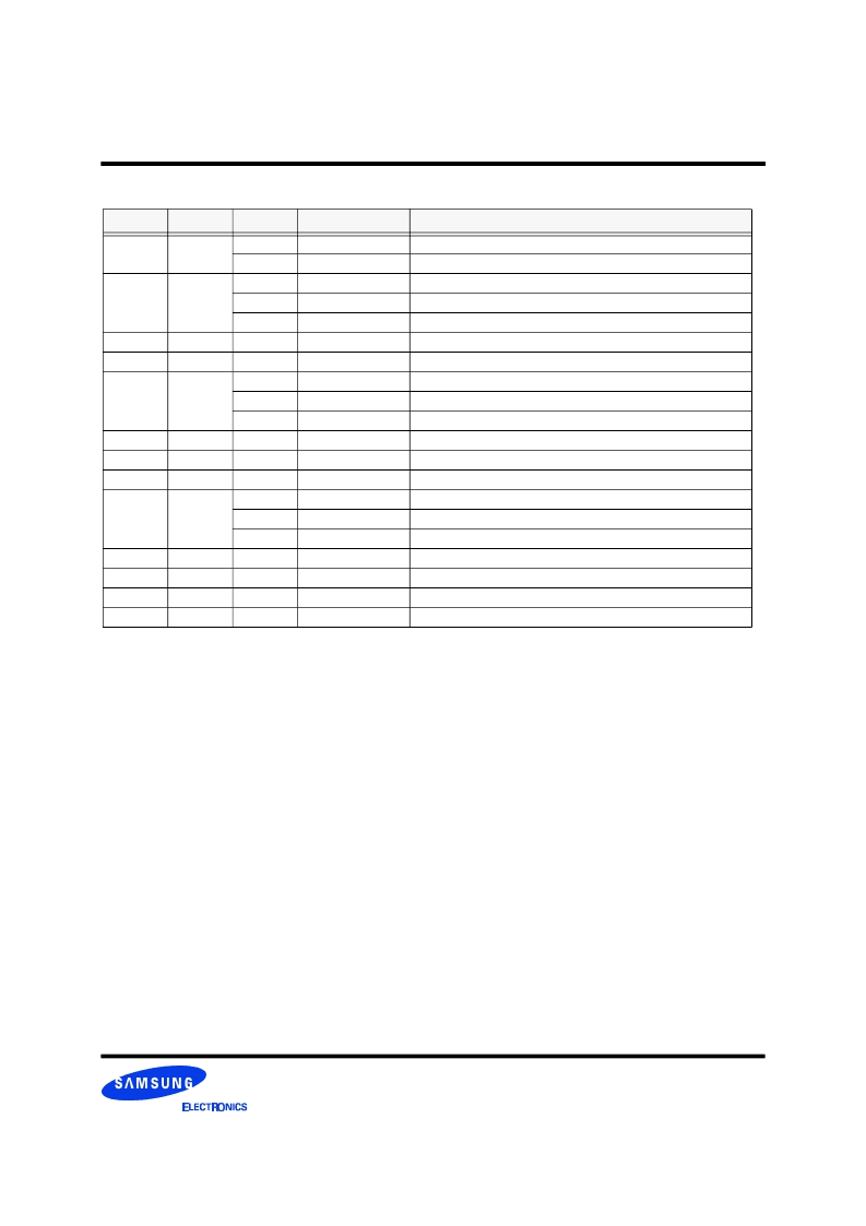
044
16
CCB
CCB
read-write, 7 bits
Current control B. Controls I
OL
output current for DQB.
ASYMB
read-write, 2 bits
Asymmetry control. Controls asymmetry of V
OL
/V
OH
swing for DQB.
045
16
NAPX
NAPXA
read-write, 5 bits
NAP exit. Specifies length of NAP exit phase A.
NAPX
read-write, 5 bits
NAP exit. Specifies length of NAP exit phase A + phase B.
DQS
read-write, 1 bits
DQ select. Selects CMD framing for NAP/PDN exit.
046
16
PDNXA
PDNXA
read-write, 13 bits
PDN exit. Specifies length of PDN exit phase A.
047
16
PDNX
PDNX
read-write, 13 bits
PDN exit. Specifies length of PDN exit phase A + phase B.
048
16
TPARM
TCAS
read-write, 2 bits
t
CAS-C
core parameter. Determines t
OFFP
datasheet parameter.
TCLS
read-write, 2 bits
t
CLS-C
core parameter. Determines t
CAC
and t
OFFP
parameters.
TCDLY0
read-write, 3 bits
t
CDLY0-C
core parameter. Programmable delay for read data.
049
16
TFRM
TFRM
read-write, 4 bits
t
FRM-C
core parameter. Determines ROW-COL packet framing interval.
04a
16
TCDLY1
TCDLY1
read-write, 3 bits
t
CDLY1-C
core parameter. Programmable delay for read data.
04c
16
TCYCLE
TCYCLE
read-write, 14 bits
t
CYCLE
datasheet parameter. Specifies cycle time in 64ps units.
04b
16
SKIP
AS
read-only, 1 bit
Autoskip value established by the SETF command.
MSE
read-write, 1 bit
Manual skip enable. Allows the MS value to override the AS value.
MS
read-write, 1 bit
Manual skip value.
04d
16-
TEST77
TEST77
read-write, 16 bits
Test register. Write with zero after SIO reset.
04e
16-
TEST78
TEST78
read-write, 16 bits
Test register. Do not read or write after SIO reset.
04f
16-
TEST79
TEST79
read-write, 16 bits
Test register. Do not read or write after SIO reset.
080
16
- 0ff
16
reserved
reserved
vendor-specific
Vendor-specific test registers. Do not read or write after SIO reset.
Table 16: Control Register Summary
SA11..SA0
Register
Field
read-write/ read-only
Description
相關(guān)PDF資料 |
PDF描述 |
|---|---|
| K4R881869M-NCK7 | 288Mbit RDRAM 512K x 18 bit x 2*16 Dependent Banks Direct RDRAMTM |
| K4R881869M-NCK8 | 288Mbit RDRAM 512K x 18 bit x 2*16 Dependent Banks Direct RDRAMTM |
| K4S280432A | 128Mbit SDRAM 8M x 4Bit x 4 Banks Synchronous DRAM LVTTL |
| K4S280432C | 128Mbit SDRAM 8M x 4Bit x 4 Banks Synchronous DRAM LVTTL |
| K4S280432F-UC | 128Mb F-die SDRAM Specification 54 TSOP-II with Pb-Free (RoHS compliant) |
相關(guān)代理商/技術(shù)參數(shù) |
參數(shù)描述 |
|---|---|
| K4R881869M-NCK7 | 制造商:SAMSUNG 制造商全稱:Samsung semiconductor 功能描述:288Mbit RDRAM 512K x 18 bit x 2*16 Dependent Banks Direct RDRAMTM |
| K4R881869M-NCK8 | 制造商:SAMSUNG 制造商全稱:Samsung semiconductor 功能描述:288Mbit RDRAM 512K x 18 bit x 2*16 Dependent Banks Direct RDRAMTM |
| K4R881869M-NCK8000 | 制造商:Samsung SDI 功能描述: |
| K4S160822D | 制造商:SAMSUNG 制造商全稱:Samsung semiconductor 功能描述:2Mx8 SDRAM 1M x 8bit x 2 Banks Synchronous DRAM LVTTL |
| K4S160822DT-G/F10 | 制造商:SAMSUNG 制造商全稱:Samsung semiconductor 功能描述:2Mx8 SDRAM 1M x 8bit x 2 Banks Synchronous DRAM LVTTL |
發(fā)布緊急采購,3分鐘左右您將得到回復(fù)。