- 您現(xiàn)在的位置:買賣IC網(wǎng) > PDF目錄374277 > K4R881869M (SAMSUNG SEMICONDUCTOR CO. LTD.) 288Mbit RDRAM 512K x 18 bit x 2*16 Dependent Banks Direct RDRAMTM PDF資料下載
參數(shù)資料
| 型號: | K4R881869M |
| 廠商: | SAMSUNG SEMICONDUCTOR CO. LTD. |
| 英文描述: | 288Mbit RDRAM 512K x 18 bit x 2*16 Dependent Banks Direct RDRAMTM |
| 中文描述: | 288Mbit RDRAM的為512k × 18位× 2 * 16屬銀行直接RDRAMTM |
| 文件頁數(shù): | 24/64頁 |
| 文件大小: | 4084K |
| 代理商: | K4R881869M |
第1頁第2頁第3頁第4頁第5頁第6頁第7頁第8頁第9頁第10頁第11頁第12頁第13頁第14頁第15頁第16頁第17頁第18頁第19頁第20頁第21頁第22頁第23頁當前第24頁第25頁第26頁第27頁第28頁第29頁第30頁第31頁第32頁第33頁第34頁第35頁第36頁第37頁第38頁第39頁第40頁第41頁第42頁第43頁第44頁第45頁第46頁第47頁第48頁第49頁第50頁第51頁第52頁第53頁第54頁第55頁第56頁第57頁第58頁第59頁第60頁第61頁第62頁第63頁第64頁
Page 22
Direct RDRAM
K4R881869M
Rev. 0.9 Jan. 2000
Preliminary
Write/Retire - Examples
The process of writing a dualoct into a sense amp of an
RDRAM bank occurs in two steps. The first step consists of
transporting the write command, write address, and write
data into the write buffer. The second step happens when the
RDRAM automatically retires the write buffer (with an
optional bytemask) into the sense amp. This two-step write
process reduces the natural turn-around delay due to the
internal bidirectional data pins.
Figure 17 (left) shows an example of this two step process.
The first COLC packet contains the WR command and an
address specifying device, bank and column. The write data
dualoct follows a time t
CWD
later. This information is loaded
into the write buffer of the specified device. The COLC
packet which follows a time t
RTR
later will retire the write
buffer. The retire will happen automatically unless (1) a
COLC packet is not framed (no COLC packet is present and
the S bit is zero), or (2) the COLC packet contains a RD
command to the same device. If the retire does not take place
at time t
RTR
after the original WR command, then the device
continues to frame COLC packets, looking for the first that
is not a RD directed to itself. A bytemask MSK(a1) may be
supplied in a COLM packet aligned with the COLC that
retires the write buffer at time t
RTR
after the WR command.
The memory controller must be aware of this two-step
write/retire process. Controller performance can be
improved, but only if the controller design accounts for
several side effects.
Figure 17 (right) shows the first of these side effects. The
first COLC packet has a WR command which loads the
address and data into the write buffer. The third COLC
causes an automatic retire of the write buffer to the sense
amp. The second and fourth COLC packets (which bracket
the retire packet) contain RD commands with the same
device, bank and column address as the original WR
command. In other words, the same dualoct address that is
written is read both before and after it is actually retired. The
first RD returns the old dualoct value from the sense amp
before it is overwritten. The second RD returns the new
dualoct value that was just written.
Figure 18 (left) shows the result of performing a RD
command to the same device in the same COLC packet slot
that would normally be used for the retire operation. The
read may be to any bank and column address; all that matters
is that it is to the same device as the WR command. The
retire operation and MSK(a1) will be delayed by a time
t
PACKET
as a result. If the RD command used the same bank
and column address as the WR command, the old data from
the sense amp would be returned. If many RD commands to
the same device were issued instead of the single one that is
shown, then the retire operation would be held off an arbi-
trarily long time. However, once a RD to another device or a
WR or NOCOP to any device is issued, the retire will take
place. Figure 18 (right) illustrates a situation in which the
controller wants to issue a WR-WR-RD COLC packet
sequence, with all commands addressed to the same device,
but addressed to any combination of banks and columns.
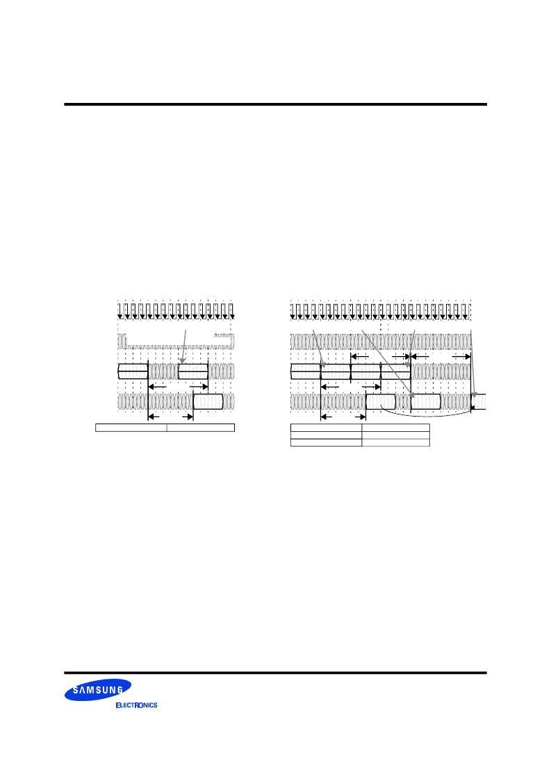
Figure 17: Normal Retire (left) and Retire/Read Ordering (right)
CTM/CFM
DQA8..0
DQB8..0
COL4
..COL0
ROW2
..ROW0
T
0
T
4
T
8
T
12
T
1
T
5
T
9
T
13
T
2
T
6
T
10
T
14
T
3
T
7
T
11
T
15
T
16
T
20
T
17
T
21
T
18
T
22
T
19
23
T
0
Transaction a: WR
a1= {Da,Ba,Ca1}
D (a1)
WR a1
CTM/CFM
DQA8..0
DQB8..0
COL4
..COL0
ROW2
..ROW0
T
4
T
8
T
12
T
1
T
5
T
9
T
13
T
2
T
6
T
10
T
14
T
3
T
7
T
11
T
15
T
16
T
20
T
17
T
21
T
18
T
22
T
19
T
23
Transaction a: WR
Transaction b: RD
Transaction c: RD
a1= {Da,Ba,Ca1}
b1= {Da,Ba,Ca1}
c1= {Da,Ba,Ca1}
retire (a1)
MSK (a1)
t
RTR
t
CWD
D (a1)
WR a1
retire (a1)
MSK (a1)
t
RTR
RD b1
RD c1
Q (b1)
t
CWD
t
CAC
This RD gets the old data
This RD gets the new data
Retire is automatic here unless:
(1) No COLC packet (S=0) or
(2) COLC packet is RD to device Da
t
CAC
Q (c1)
相關PDF資料 |
PDF描述 |
|---|---|
| K4R881869M-NbCcG6 | 288Mbit RDRAM 512K x 18 bit x 2*16 Dependent Banks Direct RDRAMTM |
| K4R881869M-NCK7 | 288Mbit RDRAM 512K x 18 bit x 2*16 Dependent Banks Direct RDRAMTM |
| K4R881869M-NCK8 | 288Mbit RDRAM 512K x 18 bit x 2*16 Dependent Banks Direct RDRAMTM |
| K4S280432A | 128Mbit SDRAM 8M x 4Bit x 4 Banks Synchronous DRAM LVTTL |
| K4S280432C | 128Mbit SDRAM 8M x 4Bit x 4 Banks Synchronous DRAM LVTTL |
相關代理商/技術參數(shù) |
參數(shù)描述 |
|---|---|
| K4R881869M-NBCCG6 | 制造商:SAMSUNG 制造商全稱:Samsung semiconductor 功能描述:288Mbit RDRAM 512K x 18 bit x 2*16 Dependent Banks Direct RDRAMTM |
| K4R881869M-NCK7 | 制造商:SAMSUNG 制造商全稱:Samsung semiconductor 功能描述:288Mbit RDRAM 512K x 18 bit x 2*16 Dependent Banks Direct RDRAMTM |
| K4R881869M-NCK8 | 制造商:SAMSUNG 制造商全稱:Samsung semiconductor 功能描述:288Mbit RDRAM 512K x 18 bit x 2*16 Dependent Banks Direct RDRAMTM |
| K4R881869M-NCK8000 | 制造商:Samsung SDI 功能描述: |
| K4S160822D | 制造商:SAMSUNG 制造商全稱:Samsung semiconductor 功能描述:2Mx8 SDRAM 1M x 8bit x 2 Banks Synchronous DRAM LVTTL |
發(fā)布緊急采購,3分鐘左右您將得到回復。