- 您現(xiàn)在的位置:買賣IC網(wǎng) > PDF目錄374277 > K4R881869M (SAMSUNG SEMICONDUCTOR CO. LTD.) 288Mbit RDRAM 512K x 18 bit x 2*16 Dependent Banks Direct RDRAMTM PDF資料下載
參數(shù)資料
| 型號(hào): | K4R881869M |
| 廠商: | SAMSUNG SEMICONDUCTOR CO. LTD. |
| 英文描述: | 288Mbit RDRAM 512K x 18 bit x 2*16 Dependent Banks Direct RDRAMTM |
| 中文描述: | 288Mbit RDRAM的為512k × 18位× 2 * 16屬銀行直接RDRAMTM |
| 文件頁(yè)數(shù): | 59/64頁(yè) |
| 文件大小: | 4084K |
| 代理商: | K4R881869M |
第1頁(yè)第2頁(yè)第3頁(yè)第4頁(yè)第5頁(yè)第6頁(yè)第7頁(yè)第8頁(yè)第9頁(yè)第10頁(yè)第11頁(yè)第12頁(yè)第13頁(yè)第14頁(yè)第15頁(yè)第16頁(yè)第17頁(yè)第18頁(yè)第19頁(yè)第20頁(yè)第21頁(yè)第22頁(yè)第23頁(yè)第24頁(yè)第25頁(yè)第26頁(yè)第27頁(yè)第28頁(yè)第29頁(yè)第30頁(yè)第31頁(yè)第32頁(yè)第33頁(yè)第34頁(yè)第35頁(yè)第36頁(yè)第37頁(yè)第38頁(yè)第39頁(yè)第40頁(yè)第41頁(yè)第42頁(yè)第43頁(yè)第44頁(yè)第45頁(yè)第46頁(yè)第47頁(yè)第48頁(yè)第49頁(yè)第50頁(yè)第51頁(yè)第52頁(yè)第53頁(yè)第54頁(yè)第55頁(yè)第56頁(yè)第57頁(yè)第58頁(yè)當(dāng)前第59頁(yè)第60頁(yè)第61頁(yè)第62頁(yè)第63頁(yè)第64頁(yè)
Page 57
Direct RDRAM
K4R881869M
Rev. 0.9 Jan. 2000
Preliminary
This circuit does not include pin coupling effects that are
often present in the packaged device. Because coupling
effects make the effective single-pin inductance L
I
, and
capacitance C
I
, a function of neighboring pins, these param-
eters are intrinsically data-dependent. For purposes of speci-
fying the device electrical loading on the Channel, the
effective L
I
and C
I
are defined as the worst-case values over
all specified operating conditions.
L
I
is defined as the effective pin inductance based on the
device pin assignment. Because the pad assignment places
each RSL signal adjacent to an AC ground (a Gnd or Vdd
pin), the effective inductance must be defined based on this
configuration. Therefore, L
I
assumes a loop with the RSL
pin adjacent to an AC ground.
C
I
is defined as the effective pin capacitance based on the
device pin assignment. It is the sum of the effective package
pin capacitance and the IO pad capacitance.
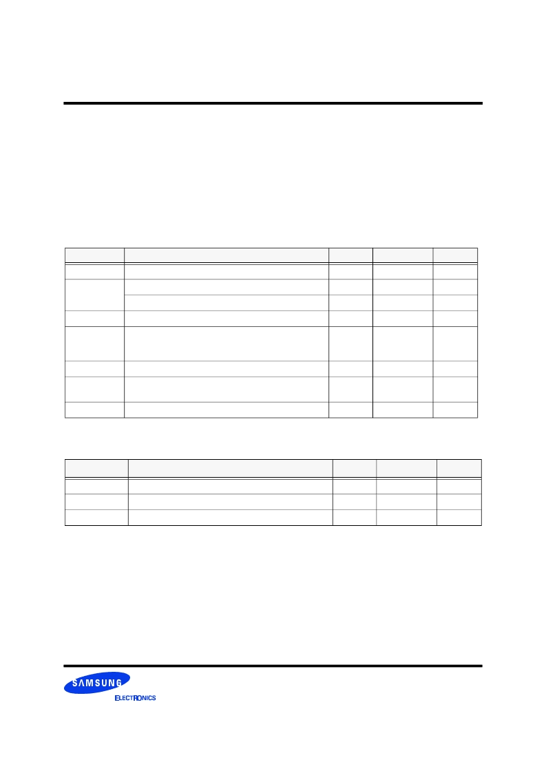
Table 25: RSL Pin Parasitics
Symbol
Parameter and Conditions - RSL pins
Min
Max
Unit
L
I
RSL effective input inductance
4.0
nH
L
12
Mutual inductance between any DQA or DQB RSL signals.
0.2
nH
Mutual inductance between any ROW or COL RSL signals.
0.6
nH
L
I
Difference in L
I
value between any RSL pins of a single device.
-
1.8
nH
C
I
RSL effective input capacitance
a
RSL effective input capacitance
a
RSL effective input capacitance
a
-800
-711
-600
2.0
2.0
2.0
2.4
2.4
2.6
pF
pF
pF
C
12
Mutual capacitance between any RSL signals.
-
0.1
pF
C
I
Difference in C
I
value between average of CTM/CFM and any
RSL pins of a single device.
-
0.06
pF
R
I
RSL effective input resistance
4
15
a. This value is a combination of the device IO circuitry and package capacitances.
Table 26: CMOS Pin Parasitics
Symbol
Parameter and Conditions - CMOS pins
Min
Max
Unit
L
I ,CMOS
CMOS effective input inductance
8.0
nH
C
I ,CMOS
CMOS effective input capacitance (SCK,CMD)
a
1.7
2.1
pF
C
I ,CMOS,SIO
CMOS effective input capacitance (SIO1, SIO0)
a
-
7.0
pF
a. This value is a combination of the device IO circuitry and package capacitances.
相關(guān)PDF資料 |
PDF描述 |
|---|---|
| K4R881869M-NbCcG6 | 288Mbit RDRAM 512K x 18 bit x 2*16 Dependent Banks Direct RDRAMTM |
| K4R881869M-NCK7 | 288Mbit RDRAM 512K x 18 bit x 2*16 Dependent Banks Direct RDRAMTM |
| K4R881869M-NCK8 | 288Mbit RDRAM 512K x 18 bit x 2*16 Dependent Banks Direct RDRAMTM |
| K4S280432A | 128Mbit SDRAM 8M x 4Bit x 4 Banks Synchronous DRAM LVTTL |
| K4S280432C | 128Mbit SDRAM 8M x 4Bit x 4 Banks Synchronous DRAM LVTTL |
相關(guān)代理商/技術(shù)參數(shù) |
參數(shù)描述 |
|---|---|
| K4R881869M-NBCCG6 | 制造商:SAMSUNG 制造商全稱:Samsung semiconductor 功能描述:288Mbit RDRAM 512K x 18 bit x 2*16 Dependent Banks Direct RDRAMTM |
| K4R881869M-NCK7 | 制造商:SAMSUNG 制造商全稱:Samsung semiconductor 功能描述:288Mbit RDRAM 512K x 18 bit x 2*16 Dependent Banks Direct RDRAMTM |
| K4R881869M-NCK8 | 制造商:SAMSUNG 制造商全稱:Samsung semiconductor 功能描述:288Mbit RDRAM 512K x 18 bit x 2*16 Dependent Banks Direct RDRAMTM |
| K4R881869M-NCK8000 | 制造商:Samsung SDI 功能描述: |
| K4S160822D | 制造商:SAMSUNG 制造商全稱:Samsung semiconductor 功能描述:2Mx8 SDRAM 1M x 8bit x 2 Banks Synchronous DRAM LVTTL |
發(fā)布緊急采購(gòu),3分鐘左右您將得到回復(fù)。