- 您現在的位置:買賣IC網 > PDF目錄374280 > K4S560432D-TC1H (SAMSUNG SEMICONDUCTOR CO. LTD.) 16M x 4bit x 4 Banks Synchronous DRAM LVTTL PDF資料下載
參數資料
| 型號: | K4S560432D-TC1H |
| 廠商: | SAMSUNG SEMICONDUCTOR CO. LTD. |
| 英文描述: | 16M x 4bit x 4 Banks Synchronous DRAM LVTTL |
| 中文描述: | 16米x 4位× 4銀行同步DRAM LVTTL |
| 文件頁數: | 11/11頁 |
| 文件大?。?/td> | 121K |
| 代理商: | K4S560432D-TC1H |
K4S560432D
CMOS SDRAM
Rev. 0.0 Jan. 2002
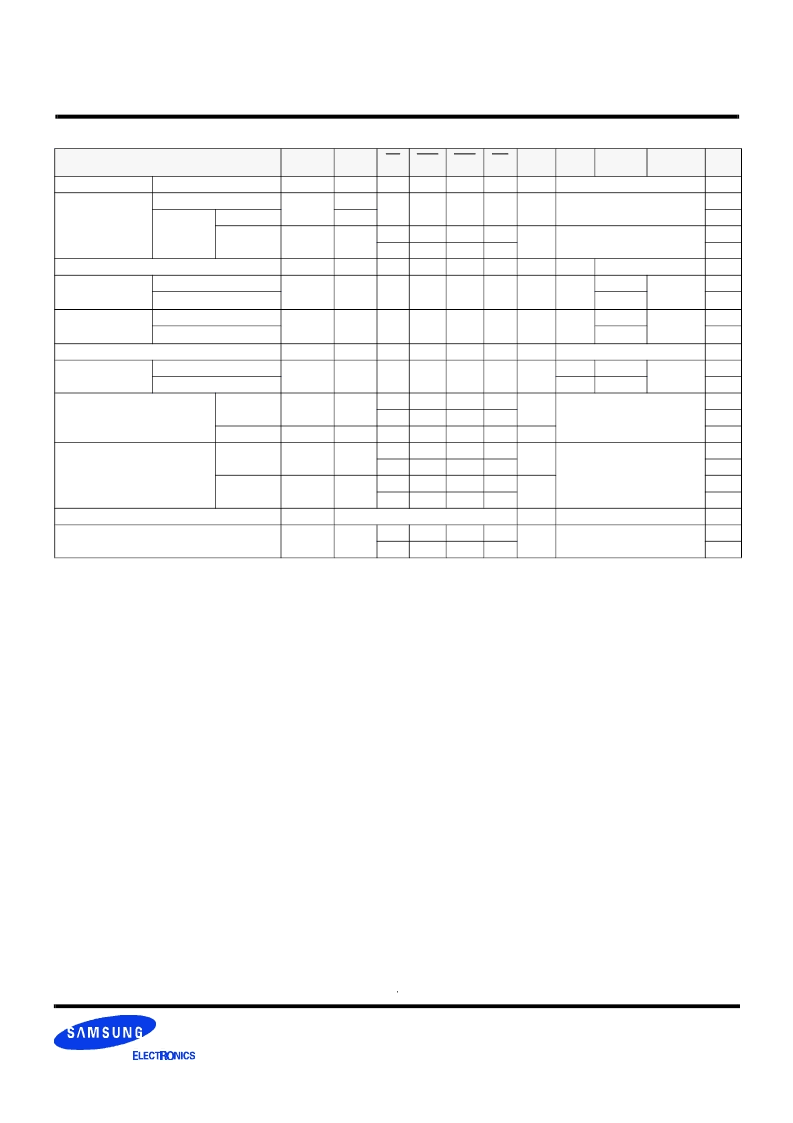
SIMPLIFIED TRUTH TABLE
(V=Valid, X=Don't care, H=Logic high, L=Logic low)
Command
CKEn-1
CKEn
CS
RAS
CAS
WE
DQM
BA
0,1
A
10
/AP
A
11,
A
12,
A
9
~ A
0
Note
Register
Mode register set
Auto refresh
H
X
H
L
L
L
L
L
X
OP code
1,2
3
3
3
3
Refresh
H
L
L
L
H
X
X
Self
refresh
Entry
Exit
L
H
L
H
L
H
X
L
H
X
H
H
X
H
X
X
Bank active & row addr.
Read &
column address
H
X
X
V
Row address
L
H
L
H
X
L
H
Auto precharge disable
Auto precharge enable
Auto precharge disable
Auto precharge enable
H
X
L
H
L
H
X
V
Column
address
(A
0
~ A
9,,
A
11
)
Column
address
(A
0
~ A
9,
A
11
)
4
4,5
4
4,5
6
Write &
column address
H
X
L
H
L
L
X
V
Burst stop
H
X
L
H
H
L
X
Precharge
Bank selection
All banks
H
X
L
L
H
L
X
V
X
X
Clock suspend or
active power down
Entry
H
L
H
L
X
H
L
H
L
X
V
X
X
H
X
V
X
X
V
X
X
H
X
V
X
V
X
X
H
X
V
X
X
Exit
L
H
X
Precharge power down mode
Entry
H
L
X
X
Exit
L
H
X
DQM
H
V
X
7
No operation command
H
X
H
L
X
H
X
H
X
H
X
X
Notes :
1. OP Code : Operand code
A
0
~ A
11
& BA
0
~ BA
1
: Program keys. (@ MRS)
2. MRS can be issued only at all banks precharge state.
A new command can be issued after 2 CLK cycles of MRS.
3. Auto refresh functions are as same as CBR refresh of DRAM.
The automatical precharge without row precharge command is meant by "Auto".
Auto/self refresh can be issued only at all banks precharge state.
4. BA
0
~ BA
1
: Bank select addresses.
If both BA
0
and BA
1
are "Low" at read, write, row active and precharge, bank A is selected.
If BA
0
is "High" and BA
1
is "Low" at read, write, row active and precharge, bank B is selected.
If BA
0
is "Low" and BA
1
is "High" at read, write, row active and precharge, bank C is selected.
If both BA
0
and BA
1
are "High" at read, write, row active and precharge, bank D is selected.
If A
10
/AP is "High" at row precharge, BA
0
and BA
1
is ignored and all banks are selected.
5. During burst read or write with auto precharge, new read/write command can not be issued.
Another bank read/write command can be issued after the end of burst.
New row active of the associated bank can be issued at t
RP
after the end of burst.
6. Burst stop command is valid at every burst length.
7. DQM sampled at positive going edge of a CLK and masks the data-in at the very CLK (Write DQM latency is 0),
but makes Hi-Z state the data-out of 2 CLK cycles after. (Read DQM latency is 2)
相關PDF資料 |
PDF描述 |
|---|---|
| K4S560432D-TC1L | 16M x 4bit x 4 Banks Synchronous DRAM LVTTL |
| K4S560432D-TC75 | 16M x 4bit x 4 Banks Synchronous DRAM LVTTL |
| K4S560432D-TC7C | 16M x 4bit x 4 Banks Synchronous DRAM LVTTL |
| K4S560432D-TL1H | 16M x 4bit x 4 Banks Synchronous DRAM LVTTL |
| K4S560432D-TL1L | 16M x 4bit x 4 Banks Synchronous DRAM LVTTL |
相關代理商/技術參數 |
參數描述 |
|---|---|
| K4S560432D-TC1L | 制造商:SAMSUNG 制造商全稱:Samsung semiconductor 功能描述:16M x 4bit x 4 Banks Synchronous DRAM LVTTL |
| K4S560432D-TC75 | 制造商:Samsung Semiconductor 功能描述:DRAM Chip SDRAM 256M-Bit 64Mx4 3.3V 54-Pin TSOP-II |
| K4S560432D-TC7C | 制造商:SAMSUNG 制造商全稱:Samsung semiconductor 功能描述:16M x 4bit x 4 Banks Synchronous DRAM LVTTL |
| K4S560432D-TL1H | 制造商:SAMSUNG 制造商全稱:Samsung semiconductor 功能描述:16M x 4bit x 4 Banks Synchronous DRAM LVTTL |
| K4S560432D-TL1L | 制造商:SAMSUNG 制造商全稱:Samsung semiconductor 功能描述:16M x 4bit x 4 Banks Synchronous DRAM LVTTL |
發(fā)布緊急采購,3分鐘左右您將得到回復。