- 您現(xiàn)在的位置:買賣IC網(wǎng) > PDF目錄374283 > K4S643232C-TC70 (SAMSUNG SEMICONDUCTOR CO. LTD.) Low Noise Precision Advanced LinCMOS(TM) Single Operational Amplifier 8-CDIP -55 to 125 PDF資料下載
參數(shù)資料
| 型號: | K4S643232C-TC70 |
| 廠商: | SAMSUNG SEMICONDUCTOR CO. LTD. |
| 英文描述: | Low Noise Precision Advanced LinCMOS(TM) Single Operational Amplifier 8-CDIP -55 to 125 |
| 中文描述: | 200萬× 32內(nèi)存為512k × 32 × 4銀行同步DRAM LVTTL |
| 文件頁數(shù): | 5/43頁 |
| 文件大小: | 1155K |
| 代理商: | K4S643232C-TC70 |
第1頁第2頁第3頁第4頁當(dāng)前第5頁第6頁第7頁第8頁第9頁第10頁第11頁第12頁第13頁第14頁第15頁第16頁第17頁第18頁第19頁第20頁第21頁第22頁第23頁第24頁第25頁第26頁第27頁第28頁第29頁第30頁第31頁第32頁第33頁第34頁第35頁第36頁第37頁第38頁第39頁第40頁第41頁第42頁第43頁
K4S643232C
CMOS SDRAM
REV. 1.1 Nov. '99
- 5 -
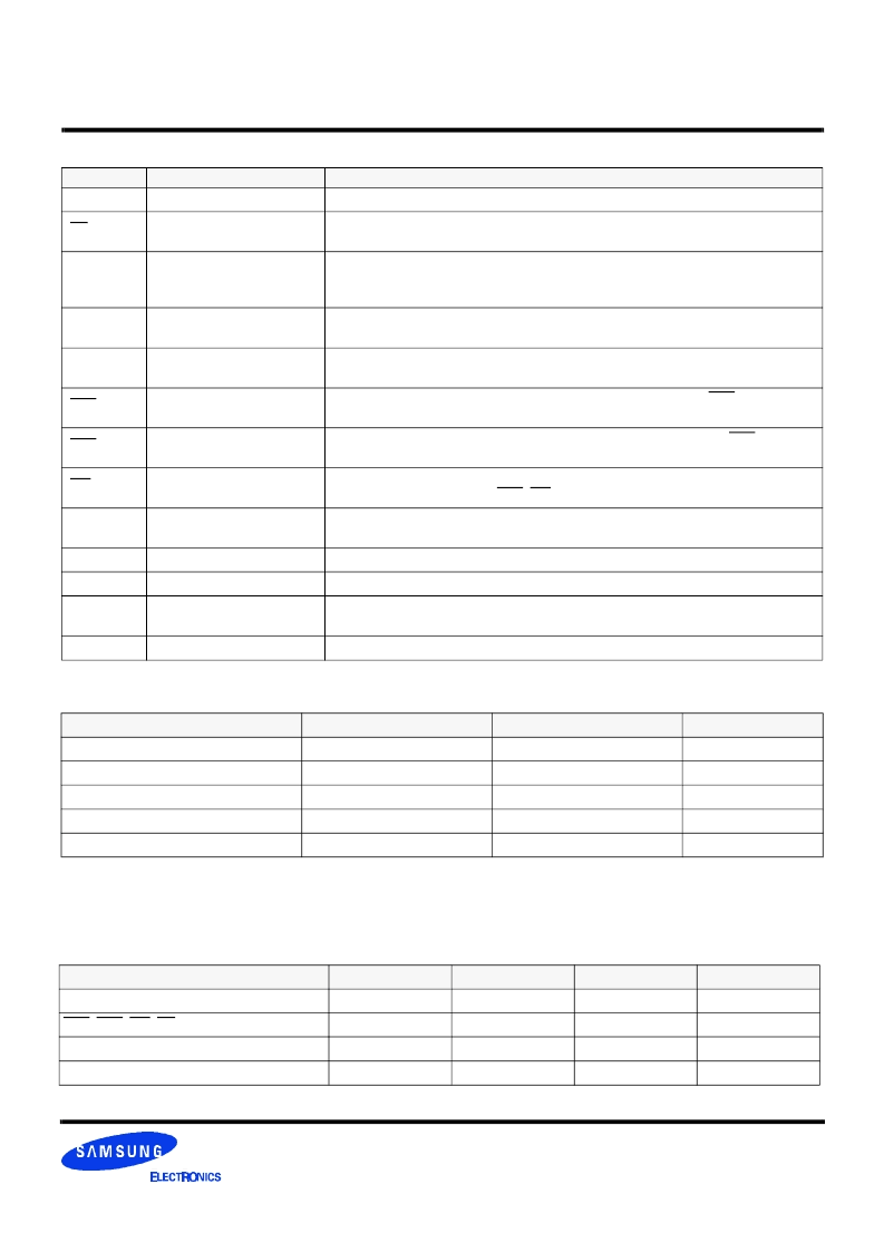
ABSOLUTE MAXIMUM RATINGS
Parameter
Symbol
Value
Unit
Voltage on any pin relative to Vss
V
IN
, V
OUT
-1.0 ~ 4.6
V
Voltage on V
DD
supply relative to Vss
V
DD
, V
DDQ
-1.0 ~ 4.6
V
Storage temperature
T
STG
-55 ~ +150
°
C
Power dissipation
P
D
1
W
Short circuit current
I
OS
50
mA
Permanent device damage may occur if "ABSOLUTE MAXIMUM RATINGS" are exceeded.
Functional operation should be restricted to recommended operating condition.
Exposure to higher than recommended voltage for extended periods of time could affect device reliability.
Note :
PIN FUNCTION DESCRIPTION
Pin
Name
Input Function
CLK
System clock
Active on the positive going edge to sample all inputs.
CS
Chip select
Disables or enables device operation by masking or enabling all inputs except
CLK, CKE and DQM.
CKE
Clock enable
Masks system clock to freeze operation from the next clock cycle.
CKE should be enabled at least one cycle prior to new command.
Disables input buffers for power down mode.
A
0
~ A
10
Address
Row/column addresses are multiplexed on the same pins.
Row address : RA
0
~ RA
10
, Column address : CA
0
~ CA
7
BA0,1
Bank select address
Selects bank to be activated during row address latch time.
Selects bank for read/write during column address latch time.
RAS
Row address strobe
Latches row addresses on the positive going edge of the CLK with RAS low.
Enables row access & precharge.
CAS
Column address strobe
Latches column addresses on the positive going edge of the CLK with CAS low.
Enables column access.
WE
Write enable
Enables write operation and row precharge.
Latches data in starting from CAS, WE active.
DQM0 ~ 3
Data input/output mask
Makes data output Hi-Z, t
SHZ
after the clock and masks the output.
Blocks data input when DQM active.
DQ
0
~
31
Data input/output
Data inputs/outputs are multiplexed on the same pins.
V
DD
/V
SS
Power supply/ground
Power and ground for the input buffers and the core logic.
V
DDQ
/V
SSQ
Data output power/ground
Isolated power supply and ground for the output buffers to provide improved noise
immunity.
NC
No Connection
This pin is recommended to be left No connection on the device.
CAPACITANCE
(V
DD
= 3.3V, T
A
= 23
°
C, f = 1MHz, V
REF
= 1.4V
±
200
mV)
Pin
Symbol
Min
Max
Unit
Clock
C
CLK
2.5
4
pF
RAS, CAS, WE, CS, CKE, DQM
C
IN
2.5
4.5
pF
Address
C
ADD
2.5
4.5
pF
DQ
0
~ DQ
31
C
OUT
4.0
6.5
pF
相關(guān)PDF資料 |
PDF描述 |
|---|---|
| K4S643232E | 2M x 32 SDRAM 512K x 32bit x 4 Banks Synchronous DRAM LVTTL |
| K4S643232E-TE70 | 2M x 32 SDRAM 512K x 32bit x 4 Banks Synchronous DRAM LVTTL(3.3V) |
| K4S643232E-TC45 | 2M x 32 SDRAM 512K x 32bit x 4 Banks Synchronous DRAM LVTTL |
| K4S643232E-TC50 | 2M x 32 SDRAM 512K x 32bit x 4 Banks Synchronous DRAM LVTTL |
| K4S643232E-TC55 | 2M x 32 SDRAM 512K x 32bit x 4 Banks Synchronous DRAM LVTTL |
相關(guān)代理商/技術(shù)參數(shù) |
參數(shù)描述 |
|---|---|
| K4S643232C-TC70000 | 制造商:Samsung SDI 功能描述:DRAM Chip SDRAM 64M-Bit 2Mx32 3.3V 86-Pin TSOP-II Tray |
| K4S643232C-TC80 | 制造商:SAMSUNG 制造商全稱:Samsung semiconductor 功能描述:2M x 32 SDRAM 512K x 32bit x 4 Banks Synchronous DRAM LVTTL |
| K4S643232C-TC8000 | 制造商:Samsung Semiconductor 功能描述: |
| K4S643232C-TL10 | 制造商:SAMSUNG 制造商全稱:Samsung semiconductor 功能描述:2M x 32 SDRAM 512K x 32bit x 4 Banks Synchronous DRAM LVTTL |
| K4S643232C-TL55 | 制造商:SAMSUNG 制造商全稱:Samsung semiconductor 功能描述:2M x 32 SDRAM 512K x 32bit x 4 Banks Synchronous DRAM LVTTL |
發(fā)布緊急采購,3分鐘左右您將得到回復(fù)。