- 您現(xiàn)在的位置:買賣IC網(wǎng) > PDF目錄374284 > K4T1G044QA (SAMSUNG SEMICONDUCTOR CO. LTD.) 1Gb A-die DDR2 SDRAM Specification PDF資料下載
參數(shù)資料
| 型號(hào): | K4T1G044QA |
| 廠商: | SAMSUNG SEMICONDUCTOR CO. LTD. |
| 英文描述: | 1Gb A-die DDR2 SDRAM Specification |
| 中文描述: | 1GB的芯片DDR2內(nèi)存規(guī)格 |
| 文件頁數(shù): | 11/28頁 |
| 文件大小: | 612K |
| 代理商: | K4T1G044QA |
第1頁第2頁第3頁第4頁第5頁第6頁第7頁第8頁第9頁第10頁當(dāng)前第11頁第12頁第13頁第14頁第15頁第16頁第17頁第18頁第19頁第20頁第21頁第22頁第23頁第24頁第25頁第26頁第27頁第28頁
Page 11 of 28
Rev. 1.1 Aug. 2005
DDR2 SDRAM
1G A-die DDR2 SDRAM
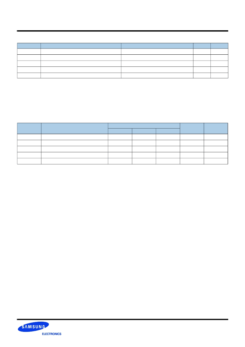
Absolute Maximum DC Ratings
Note :
1. Stresses greater than those listed under “Absolute Maximum Ratings” may cause permanent damage to the device. This is a stress rating only and
functional operation of the device at these or any other conditions above those indicated in the operational sections of this specification is not implied.
Exposure to absolute maximum rating conditions for extended periods may affect reliability.
2. Storage Temperature is the case surface temperature on the center/top side of the DRAM. For the measurement conditions, please refer to JESD51-2
standard.
AC & DC Operating Conditions
Recommended DC Operating Conditions (SSTL - 1.8)
Note : There is no specific device V
DD
supply voltage requirement for SSTL-1.8 compliance. However under all conditions V
DDQ
must be less than or equal
to V
DD
.
1. The value of V
REF
may be selected by the user to provide optimum noise margin in the system. Typically the value of V
REF
is expected to be about 0.5
x V
DDQ
of the transmitting device and V
REF
is expected to track variations in V
DDQ
.
2. Peak to peak AC noise on V
REF
may not exceed +/-2% V
REF
(DC).
3. V
TT
of transmitting device must track V
REF
of receiving device.
4. AC parameters are measured with V
DD
, V
DDQ
and V
DDL
tied together.
Symbol
Parameter
Rating
Units
Notes
V
DD
Voltage on V
DD
pin relative to V
SS
- 1.0 V ~ 2.3 V
V
1
V
DDQ
Voltage on V
DDQ
pin relative to V
SS
- 0.5 V ~ 2.3 V
V
1
V
DDL
Voltage on V
DDL
pin relative to V
SS
- 0.5 V ~ 2.3 V
V
1
V
IN,
V
OUT
Voltage on any pin relative to V
SS
- 0.5 V ~ 2.3 V
V
1
T
STG
Storage Temperature
-55 to +100
°
C
1, 2
Symbol
Parameter
Rating
Units
Notes
Min.
Typ.
Max.
V
DD
Supply Voltage
1.7
1.8
1.9
V
V
DDL
Supply Voltage for DLL
1.7
1.8
1.9
V
4
V
DDQ
Supply Voltage for Output
1.7
1.8
1.9
V
4
V
REF
Input Reference Voltage
0.49*V
DDQ
0.50*V
DDQ
0.51*V
DDQ
mV
1,2
V
TT
Termination Voltage
V
REF
-0.04
V
REF
V
REF
+0.04
V
3
相關(guān)PDF資料 |
PDF描述 |
|---|---|
| K4T1G044QA-ZCD5 | 1Gb A-die DDR2 SDRAM Specification |
| K4T1G044QA-ZCE6 | 1Gb A-die DDR2 SDRAM Specification |
| K4T1G084QA-ZCD5 | 1Gb A-die DDR2 SDRAM Specification |
| K4T1G084QA-ZCE6 | 1Gb A-die DDR2 SDRAM Specification |
| K4T1G164QA-ZCD5 | 1Gb A-die DDR2 SDRAM Specification |
相關(guān)代理商/技術(shù)參數(shù) |
參數(shù)描述 |
|---|---|
| K4T1G044QA-ZCD5 | 制造商:SAMSUNG 制造商全稱:Samsung semiconductor 功能描述:1Gb A-die DDR2 SDRAM Specification |
| K4T1G044QA-ZCD5000 | 制造商:Samsung Semiconductor 功能描述:1GB DDR SDRAM (DDR2) X4 BOC - Trays |
| K4T1G044QA-ZCE6 | 制造商:SAMSUNG 制造商全稱:Samsung semiconductor 功能描述:1Gb A-die DDR2 SDRAM Specification |
| K4T1G044QC | 制造商:SAMSUNG 制造商全稱:Samsung semiconductor 功能描述:1Gb C-die DDR2 SDRAM Specification |
| K4T1G044QE | 制造商:SAMSUNG 制造商全稱:Samsung semiconductor 功能描述:1Gb E-die DDR2 SDRAM |
發(fā)布緊急采購,3分鐘左右您將得到回復(fù)。