- 您現(xiàn)在的位置:買賣IC網(wǎng) > PDF目錄374293 > K7D323674A-HC40 (SAMSUNG SEMICONDUCTOR CO. LTD.) 32Mb A-die DDR SRAM Specification PDF資料下載
參數(shù)資料
| 型號: | K7D323674A-HC40 |
| 廠商: | SAMSUNG SEMICONDUCTOR CO. LTD. |
| 英文描述: | 32Mb A-die DDR SRAM Specification |
| 中文描述: | 32兆甲芯片的DDR SRAM的規(guī)范 |
| 文件頁數(shù): | 11/19頁 |
| 文件大小: | 494K |
| 代理商: | K7D323674A-HC40 |
Rev 1.4
Oct. 2005
1Mx36 & 2Mx18 SRAM
- 11
K7D321874A
K7D323674A
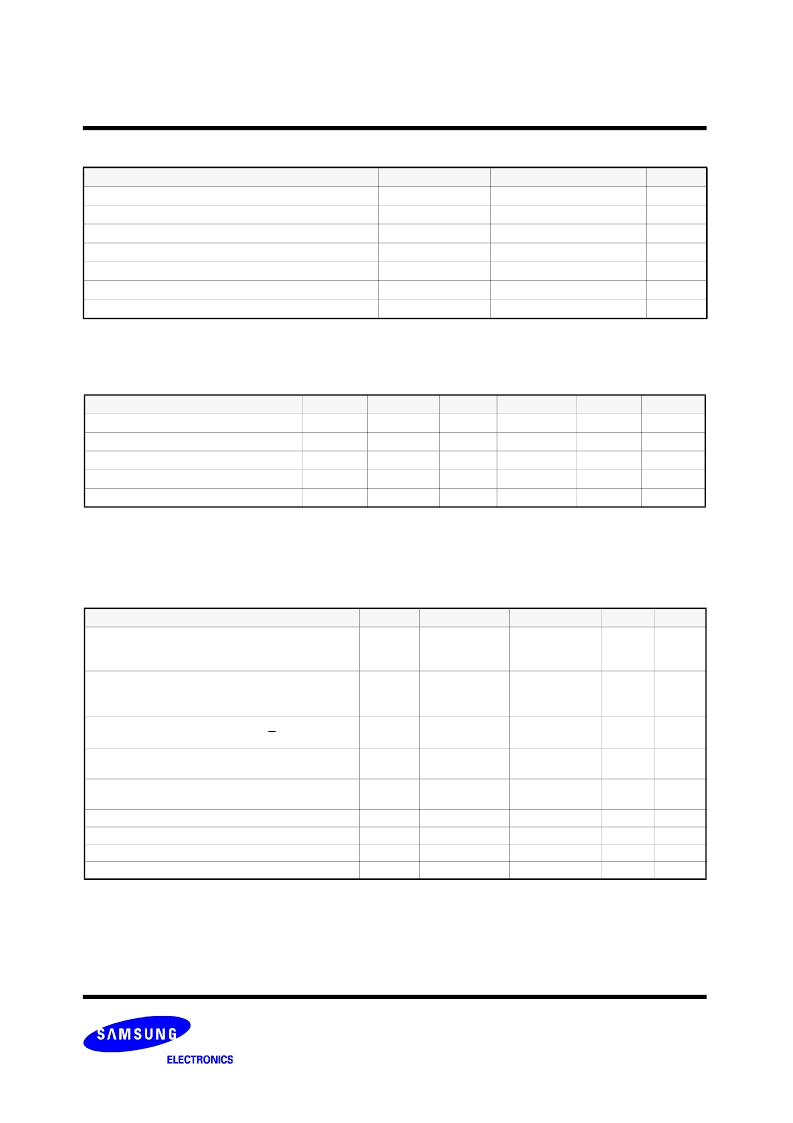
RECOMMENDED DC OPERATING CONDITIONS
NOTE
:1. These are DC test criteria. DC design criteria is V
REF
±
50mV. The AC V
IH
/V
IL
levels are defined separately for measuring
timing parameters.
2. V
IH
(Max)DC=
V
DDQ
+0.3, V
IH
(Max)AC=
2.6
V (2.1V for DQs) (pulse width
≤
20% of cycle time).
3. V
IL
(Min)DC=
-
0.3V, V
IL
(Min)AC=-1.0V (-0.5V for DQs) (pulse width
≤
20% of cycle time).
Parameter
Symbol
Min
Typ
Max
Unit
Note
Core Power Supply Voltage
V
DD
1.7
2.5
2.6
V
Output Power Supply Voltage
V
DDQ
1.4
1.5
1.9
V
Input High Level Voltage
V
IH
V
REF
+0.1
-
V
DDQ
+0.3
V
1, 2
Input Low Level Voltage
V
IL
-0.3
-
V
REF
-0.1
V
1, 3
Input Reference Voltage
V
REF
0.68
0.75
1.0
V
ABSOLUTE MAXIMUM RATINGS
NOTE
: Power Dissipation Capability will be dependent upon package characteristics and use environment. See enclosed thermal impedance data.
Stresses greater than those listed under " Absolute Maximum Ratings" may cause permanent damage to the device. This is a stress rating only
and functional operation of the device at these or any other conditions above those indicated in the operating sections of this specification is not
implied. Exposure to absolute maximum rating conditions for extended periods may affect reliability.
Parameter
Symbol
Value
Unit
Core Supply Voltage Relative to V
SS
V
DD
-0.5 to 3.13
V
Output Supply Voltage Relative to V
SS
V
DDQ
-0.5 to 2.3
V
Voltage on any pin Relative to V
SS
V
IN
-0.5 to V
DDQ
+0.5 (2.3V
MAX
)
V
Output Short-Circuit Current(per I/O)
I
OUT
25
mA
Storage Temperature
T
STR
-55 to 125
°
C
Maxmum Junction Temperature
T
J
110
°
C
Maxmum Power Dissipation
P
D
3.0
W
DC CHARACTERISTICS
NOTE
:1. Minimum cycle. I
OUT
=0mA.
2. 50% read cycles.
3. |I
OH
|=(V
DDQ
/2)/(RQ/5)
±
15% @V
OH
=V
DDQ
/2 for 175
≤
RQ
≤
300
.
4. |I
OL
|=(V
DDQ
/2)/(RQ/5)
±
15% @V
OL
=V
DDQ
/2 for 175
≤
RQ
≤
300
.
Parameter
Symbol
Min
Max
Unit
Note
Average Power Supply Operating Current(x36)
(Cycle time = t
KHKH
min)
I
DD40
I
DD37
I
DD33
-
960
940
900
mA
1,2
Average Power Supply Operating Current(x18)
(Cycle time = t
KHKH
min)
I
DD40
I
DD37
I
DD33
-
910
890
850
mA
1,2
Stop Clock Standby Current
(V
IN
=V
DD
-0.2V or 0.2V fixed, K=Low, K=High)
I
SB1
-
300
mA
1
Input Leakage Current
(V
IN
=V
SS
or V
DDQ
)
I
LI
-3
3
μ
A
Output Leakage Current
(V
OUT
=V
SS
or V
DDQ
)
I
LO
-5
5
μ
A
Output High Voltage(Programmable Impedance Mode)
V
OH1
V
DDQ
/2
V
DDQ
V
3
Output Low Voltage(Programmable Impedance Mode)
V
OL1
V
SS
V
DDQ
/2
V
4
Output High Voltage(I
OH
=-0.1mA)
V
OH2
V
DDQ
-0.2
V
DDQ
V
Output Low Voltage(I
OL
=0.1mA)
V
OL2
V
SS
0.2
V
相關(guān)PDF資料 |
PDF描述 |
|---|---|
| K7D323674A-HGC33 | 32Mb A-die DDR SRAM Specification |
| K7D323674A-HGC37 | 32Mb A-die DDR SRAM Specification |
| K7D323674A-HGC40 | 32Mb A-die DDR SRAM Specification |
| K7D801871B-HC25 | 256Kx36 & 512Kx18 SRAM |
| K7D801871B-HC30 | 256Kx36 & 512Kx18 SRAM |
相關(guān)代理商/技術(shù)參數(shù) |
參數(shù)描述 |
|---|---|
| K7D323674A-HGC33 | 制造商:SAMSUNG 制造商全稱:Samsung semiconductor 功能描述:32Mb A-die DDR SRAM Specification |
| K7D323674A-HGC37 | 制造商:SAMSUNG 制造商全稱:Samsung semiconductor 功能描述:32Mb A-die DDR SRAM Specification |
| K7D323674A-HGC40 | 制造商:SAMSUNG 制造商全稱:Samsung semiconductor 功能描述:32Mb A-die DDR SRAM Specification |
| K7D323674C | 制造商:SAMSUNG 制造商全稱:Samsung semiconductor 功能描述:1Mx36 & 2Mx18 SRAM |
| K7D801871B-HC25 | 制造商:SAMSUNG 制造商全稱:Samsung semiconductor 功能描述:256Kx36 & 512Kx18 SRAM |
發(fā)布緊急采購,3分鐘左右您將得到回復(fù)。