- 您現(xiàn)在的位置:買賣IC網(wǎng) > PDF目錄374293 > K7D803671B-HC25 (SAMSUNG SEMICONDUCTOR CO. LTD.) 256Kx36 & 512Kx18 SRAM PDF資料下載
參數(shù)資料
| 型號: | K7D803671B-HC25 |
| 廠商: | SAMSUNG SEMICONDUCTOR CO. LTD. |
| 英文描述: | 256Kx36 & 512Kx18 SRAM |
| 中文描述: | 256Kx36 |
| 文件頁數(shù): | 2/16頁 |
| 文件大小: | 270K |
| 代理商: | K7D803671B-HC25 |
Rev 4.0
256Kx36 & 512Kx18 SRAM
- 2 -
January. 2002
K7D801871B
K7D803671B
PIN DESCRIPTION
Pin Name
Pin Description
Pin Name
Pin Description
K, K
Differential Clocks
ZQ
Output Driver Impedance Control Input
SA
Synchronous Address Input
TCK
JTAG Test Clock
SA
0
, SA
1
Synchronous Burst Address Input (SA
0
= LSB)
TMS
JTAG Test Mode Select
DQ
Synchronous Data I/O
TDI
JTAG Test Data Input
CQ, CQ
Differential Output Echo Clocks
TDO
JTAG Test Data Output
B
1
Load External Address
V
REF
HSTL Input Reference Voltage
B
2
Burst R/W Enable
V
DD
Power Supply
B
3
Single/Double Data Selection
V
DDQ
Output Power Supply
G
Asynchronous Output Enable
V
SS
GND
LBO
Linear Burst Order
NC
No Connection
FEATURES
256Kx36 or 512Kx18 Organizations.
Maximum Frequency : 370MHz (Data Rate : 740Mbps)
2.5V V
DD
/1.5V V
DDQ
(2.0V max V
DDQ
).
HSTL Input and Outputs.
Single Differential HSTL Clock.
Synchronous Pipeline Mode of Operation with Self-Timed Late Write.
Free Running Active High and Active Low Echo Clock Output Pin.
Asynchronous Output Enable.
Registered Addresses, Burst Control and Data Inputs.
Registered Outputs.
Single and Double Data Rate Burst Read and Write.
Burst Count Controllable With Max Burst Length of 4
Interleved and Linear Burst mode support
Bypass Operation Support
Programmable Impedance Output Drivers.
JTAG Boundary Scan (subset of IEEE std. 1149.1)
153(9x17) Pin Ball Grid Array Package(14mm x 22mm).
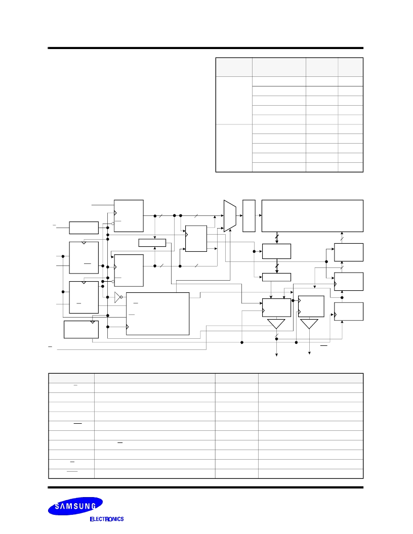
FUNCTIONAL BLOCK DIAGRAM
K,K
B
1
B
3
B
2
G
Register
CE
Memory Array
256Kx36
or
(512Kx18)
Data Out
Data In
Advance
Control
SD/DD
Clock
Buffer
Synchronous
Select
&
R/W control
Internal
Clock
Generator
CE
R/W
LD
Data Output Strobe
Data Output Enable
State Machine
Strobe_out
S/A Array
2 : 1 MUX
Data In
Register
(2 stage)
Write Buffer
W/D
Array
Echo Clock
Output
36(or 18)x2
36(or 18)x2
36(or18)x2
36(or18)x2
XDIN
CQ,CQ
DQ
36(or 18)
Output
Buffer
Write
Address
CE
Burst
Counter
Register
(2 stage)
Address
Comparator
2:1
MUX
Dec.
18(or 19)
16(or 17)
16(or 17)
18(or 19)
(Burst Write
Address)
SA[0:17]( or SA[0:18])
(Burst Address)
NOTE
: *Access time equals
t
KXCH/
t
KXCL
Organization
Part Number
Maximum
Frequency
Access
Time
256Kx36
K7D803671B-HC37
370MHz
1.7*
K7D803671B-HC35
357MHz
1.7*
K7D803671B-HC33
333MHz
1.7*
K7D803671B-HC30
300MHz
1.9*
K7D803671B-HC25
250MHz
2.0*
512Kx18
K7D801871B-HC37
370MHz
1.7*
K7D801871B-HC35
357MHz
1.7*
K7D801871B-HC33
333MHz
1.7*
K7D801871B-HC30
300MHz
1.9*
K7D801871B-HC25
250MHz
2.0*
相關(guān)PDF資料 |
PDF描述 |
|---|---|
| K7D803671B-HC30 | 256Kx36 & 512Kx18 SRAM |
| K7D803671B-HC33 | 256Kx36 & 512Kx18 SRAM |
| K7D803671B-HC35 | 256Kx36 & 512Kx18 SRAM |
| K7D803671B-HC37 | 256Kx36 & 512Kx18 SRAM |
| K7I321882M | 1Mx36 & 2Mx18 DDRII CIO b2 SRAM |
相關(guān)代理商/技術(shù)參數(shù) |
參數(shù)描述 |
|---|---|
| K7D803671B-HC25000 | 制造商:Samsung SDI 功能描述: 制造商:Samsung Semiconductor 功能描述: |
| K7D803671B-HC25T00 | 制造商:Samsung Semiconductor 功能描述:8MSYNCDOUBLE DATA RATE SRAMX36BGA, T/R - Tape and Reel |
| K7D803671B-HC30 | 制造商:SAMSUNG 制造商全稱:Samsung semiconductor 功能描述:256Kx36 & 512Kx18 SRAM |
| K7D803671B-HC33 | 制造商:SAMSUNG 制造商全稱:Samsung semiconductor 功能描述:256Kx36 & 512Kx18 SRAM |
| K7D803671B-HC33000 | 制造商:Samsung 功能描述:8MSYNCDOUBLE DATA RATE SRAMX36BGA - Bulk |
發(fā)布緊急采購,3分鐘左右您將得到回復(fù)。