- 您現(xiàn)在的位置:買賣IC網(wǎng) > PDF目錄374293 > K7M803625A (SAMSUNG SEMICONDUCTOR CO. LTD.) Evaluation Module for TPS650732 5-Channel Power Management IC PDF資料下載
參數(shù)資料
| 型號: | K7M803625A |
| 廠商: | SAMSUNG SEMICONDUCTOR CO. LTD. |
| 英文描述: | Evaluation Module for TPS650732 5-Channel Power Management IC |
| 中文描述: | 256Kx36 |
| 文件頁數(shù): | 7/20頁 |
| 文件大小: | 321K |
| 代理商: | K7M803625A |
256Kx36 & 512Kx18 Flow-Through N
t
RAM
TM
- 7 -
Rev 1.0
July 2000
K7M801825A
K7M803625A
FUNCTION DESCRIPTION
The K7M803625A and K7M801825A are N
t
RAM
TM
designed to sustain 100% bus bandwidth by eliminating turnaround cycle when
there is transition from Read to Write, or vice versa.
All inputs (with the exception of OE, LBO and ZZ) are synchronized to rising clock edges.
All read, write and deselect cycles are initiated by the ADV input. Subsequent burst addresses can be internally generated by the
burst advance pin (ADV). ADV should be driven to Low once the device has been deselected in order to load a new address for next
operation.
Clock Enable(CKE) pin allows the operation of the chip to be suspended as long as necessary. When CKE is high, all synchronous
inputs are ignored and the internal device registers will hold their previous values.
N
t
RAM
TM
latches external address and initiates a cycle, when CKE, ADV are driven to low and all three chip enables(CS
1
, CS
2
, CS
2
)
are active .
Output Enable(OE) can be used to disable the output at any given time.
Read operation is initiated when at the rising edge of the clock, the address presented to the address inputs are latched in the
address register, CKE is driven low, all three chip enables(CS
1
, CS
2
, CS
2
) are active, the write enable input signals WE are driven
high, and ADV driven low. Data appears at the outputs within the same clock cycle as the address for the data. Also during read
operation OE must be driven low for the device to drive out the requested data.
Write operation occurs when WE is driven low at the rising edge of the clock. BW[d:a] can be used for byte write operation. The Flow
Through N
t
RAM
TM
uses a late write cycle to utilize 100% of the bandwidth.
At the first rising edge of the clock, WE and address are registered, and the data associated with that address is required one cycle
later.
Subsequent addresses are generated by ADV High for the burst access as shown below. The starting point of the burst seguence is
provided by the external address. The burst address counter wraps around to its initial state upon completion.
The burst sequence is determined by the state of the LBO pin. When this pin is low, linear burst sequence is selected.
And when this pin is high, Interleaved burst sequence is selected.
During normal operation, ZZ must be driven low. When ZZ is driven high, the SRAM will enter a Power Sleep Mode after 2 cycles. At
this time, internal state of the SRAM is preserved. When ZZ returns to low, the SRAM normally operates after 2 cycles of wake up
time.
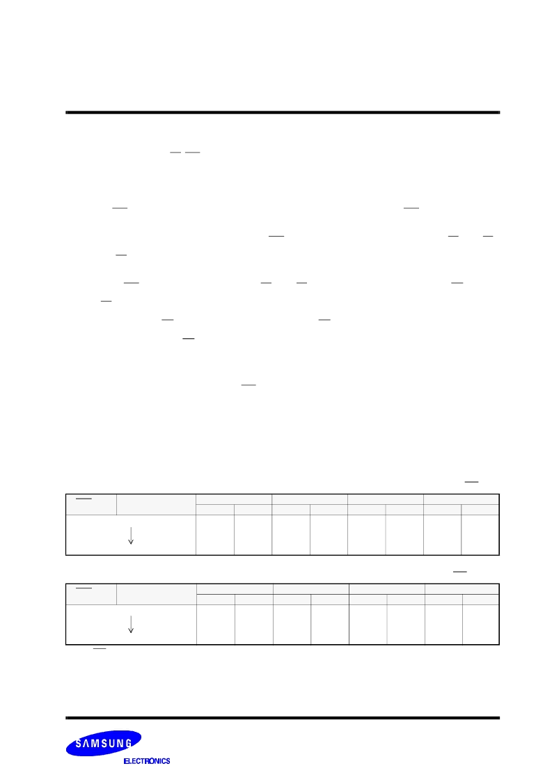
BURST SEQUENCE TABLE
(Interleaved Burst, LBO=High)
LBO PIN
HIGH
Case 1
Case 2
Case 3
Case 4
A
1
0
0
1
1
A
0
0
1
0
1
A
1
0
0
1
1
A
0
1
0
1
0
A
1
1
1
0
0
A
0
0
1
0
1
A
1
1
1
0
0
A
0
1
0
1
0
First Address
Fourth Address
BQ TABLE
(Linear Burst, LBO=Low)
Case 1
A
1
A
0
First Address
0
0
1
1
1
Note
:
1. LBO pin must be tied to High or Low, and Floating State must not be allowed
.
LBO PIN
LOW
Case 2
Case 3
Case 4
A
1
0
1
1
0
A
0
1
0
1
0
A
1
1
1
0
0
A
0
0
1
0
1
A
1
1
0
0
1
A
0
1
0
1
0
Fourth Address
0
1
0
相關(guān)PDF資料 |
PDF描述 |
|---|---|
| K7M801825B | 256Kx36 & 512Kx18-Bit Flow Through NtRAM |
| K7M803625B | 256Kx36 & 512Kx18-Bit Flow Through NtRAM |
| K7N161801M | 512Kx36 & 1Mx18-Bit Pipelined NtRAM TM |
| K7N163601M | 512Kx36 & 1Mx18-Bit Pipelined NtRAM TM |
| K7N161845M | 512Kx36 & 1Mx18-Bit Pipelined NtRAMTM |
相關(guān)代理商/技術(shù)參數(shù) |
參數(shù)描述 |
|---|---|
| K7M803625B | 制造商:SAMSUNG 制造商全稱:Samsung semiconductor 功能描述:256Kx36 & 512Kx18-Bit Flow Through NtRAM |
| K7M803625B_06 | 制造商:SAMSUNG 制造商全稱:Samsung semiconductor 功能描述:256Kx36 & 512Kx18 Flow-Through NtRAM |
| K7M803625B-QC65 | 制造商:SAMSUNG 制造商全稱:Samsung semiconductor 功能描述:256Kx36 & 512Kx18-Bit Pipelined NtRAMTM |
| K7M803625B-QC65/75 | 制造商:SAMSUNG 制造商全稱:Samsung semiconductor 功能描述:256Kx36 & 512Kx18-Bit Flow Through NtRAM |
| K7M803625B-QC75 | 制造商:SAMSUNG 制造商全稱:Samsung semiconductor 功能描述:256Kx36 & 512Kx18-Bit Pipelined NtRAM |
發(fā)布緊急采購,3分鐘左右您將得到回復(fù)。