- 您現(xiàn)在的位置:買賣IC網(wǎng) > PDF目錄374294 > K7N401801M (SAMSUNG SEMICONDUCTOR CO. LTD.) TPS55065EVM Evaluation Module PDF資料下載
參數(shù)資料
| 型號(hào): | K7N401801M |
| 廠商: | SAMSUNG SEMICONDUCTOR CO. LTD. |
| 英文描述: | TPS55065EVM Evaluation Module |
| 中文描述: | 128K × 36至 |
| 文件頁數(shù): | 2/17頁 |
| 文件大?。?/td> | 273K |
| 代理商: | K7N401801M |
K7N403601M
K7N401801M
128Kx36 & 256Kx18 Pipelined N
t
RAM
TM
- 2 -
Rev 3.0
May 1999
128Kx36 & 256Kx18-Bit Pipelined N
t
RAM
TM
The K7N403601M and K7N401801M are 4,718,592 bits Syn-
chronous Static SRAMs.
The N
t
RAM
TM
, or No Turnaround Random Access Memory uti-
lizes all the bandwidth in any combination of operating cycles.
Address, data inputs, and all control signals except output
enable and linear burst order are synchronized to input clock.
Burst order control must be tied "High or Low".
Asynchronous inputs include the sleep mode enable(ZZ).
Output Enable controls the outputs at any given time.
Write cycles are internally self-timed and initiated by the rising
edge of the clock input. This feature eliminates complex off-chip
write pulse generation
and provides increased timing flexibility for incomming signals.
For read cycles, pipelined SRAM output data is temporarily
stored by an edge trigered output register and then released to
the output bufferes at the next rising edge of clock.
The K7N403601M and K7N401801M are implemented with
SAMSUNG
′
s high performance CMOS technology and is avail-
able in 100pin TQFP packages. Multiple power and ground pins
minimize ground bounce.
GENERAL DESCRIPTION
FEATURES
3.3V+0.165V/-0.165V Power Supply.
I/O Supply Voltage 3.3V+0.165V/-0.165V for 3.3V I/O
or 2.5V+0.4V/-0.125V for 2.5V I/O
.
Byte Writable Function.
Enable clock and suspend operation.
Single READ/WRITE control pin.
Self-Timed Write Cycle.
Three Chip Enable for simple depth expansion with no data
contention
Α
interleaved burst or a linear burst mode.
Asynchronous output enable control.
Power Down mode.
TTL-Level Three-State Outputs.
100-TQFP-1420A Package.
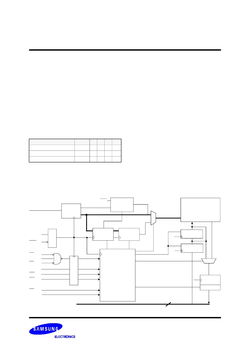
LOGIC BLOCK DIAGRAM
FAST ACCESS TIMES
PARAMETER
Symbol -15 -13 -10 Unit
Cycle Time
t
CYC
6.7
7.5
10
ns
Clock Access Time
t
CD
3.8
4.2 5.0
ns
Output Enable Access Time
t
OE
3.8
4.2 5.0
ns
WE
BW
(x=a,b,c,d or a,b)
CLK
CKE
CS
1
CS
2
CS
2
ADV
OE
ZZ
DQa
~ DQd
or
DQa
0
~ DQb
8
DQPa ~ DQPd
ADDRESS
REGISTER
ADDRESS
REGISTER
C
L
A
′
0
~A
′
1
36 or 18
OUTPUT
REGISTER
BUFFER
DATA-IN
REGISTER
DATA-IN
REGISTER
K
K
K
BURST
ADDRESS
COUNTER
WRITE
ADDRESS
REGISTER
WRITE
CONTROL
LOGIC
C
R
K
A [0:16]or
A [0:17]
LBO
A
0
~A
1
A
2
~A
16
or
A
2
~A
17
128Kx36 , 256Kx18
MEMORY
ARRAY
N
t
RAM
TM
and No Turnaround Random Access Memory are trademarks of Samsung,
and its architecture and functionalities are supported by NEC and Toshiba.
相關(guān)PDF資料 |
PDF描述 |
|---|---|
| K7N403601M | TPS54162EVM Evaluation Module |
| K7N401809B-QC20 | 128Kx36 & 256Kx18 Pipelined NtRAMTM |
| K7N403601B-QC13 | 128Kx36 & 256Kx18 Pipelined NtRAMTM |
| K7N403609B-QC20 | 128Kx36 & 256Kx18 Pipelined NtRAMTM |
| K7N403609B | 128Kx36 & 256Kx18 Pipelined NtRAMTM |
相關(guān)代理商/技術(shù)參數(shù) |
參數(shù)描述 |
|---|---|
| K7N401801M-QC1500 | 制造商:Samsung SDI 功能描述: |
| K7N401809B | 制造商:SAMSUNG 制造商全稱:Samsung semiconductor 功能描述:128Kx36 & 256Kx18 Pipelined NtRAM |
| K7N401809B-QC20 | 制造商:SAMSUNG 制造商全稱:Samsung semiconductor 功能描述:128Kx36 & 256Kx18 Pipelined NtRAMTM |
| K7N403601A | 制造商:SAMSUNG 制造商全稱:Samsung semiconductor 功能描述:128Kx36 & 256Kx18-Bit Pipelined NtRAMTM |
| K7N403601B | 制造商:SAMSUNG 制造商全稱:Samsung semiconductor 功能描述:128Kx36 & 256Kx18 Pipelined NtRAM |
發(fā)布緊急采購,3分鐘左右您將得到回復(fù)。