- 您現(xiàn)在的位置:買賣IC網(wǎng) > PDF目錄374294 > K7P403622B-HC25 (SAMSUNG SEMICONDUCTOR CO. LTD.) 128Kx36 & 256Kx18 Synchronous Pipelined SRAM PDF資料下載
參數(shù)資料
| 型號: | K7P403622B-HC25 |
| 廠商: | SAMSUNG SEMICONDUCTOR CO. LTD. |
| 英文描述: | 128Kx36 & 256Kx18 Synchronous Pipelined SRAM |
| 中文描述: | 128K × 36至 |
| 文件頁數(shù): | 2/13頁 |
| 文件大小: | 280K |
| 代理商: | K7P403622B-HC25 |
Rev 1.2
Jul. 2003
- 2 -
K7P401822B
128Kx36 & 256Kx18 SRAM
K7P403622B
PIN DESCRIPTION
Pin Name
Pin Description
Pin Name
Pin Description
K, K
Differential Clocks
ZZ
Asynchronous Power Down
SAn
Synchronous Address Input
G
Asynchronous Output Enable
DQn
Bi-directional Data Bus
TCK
JTAG Test Clock
SS
Synchronous Select
TMS
JTAG Test Mode Select
SW
Synchronous Global Write Enable
TDI
JTAG Test Data Input
SWa
Synchronous Byte a Write Enable
TDO
JTAG Test Data Output
SWb
Synchronous Byte b Write Enable
V
DD
Power Supply
SWc
Synchronous Byte c Write Enable
V
DDQ
Output Power Supply
SWd
Synchronous Byte d Write Enable
V
SS
GND
M
1
, M
2
Read Protocol Mode Pins (M
1
=V
SS
, M
2
=V
DD
)
NC
No Connection
128Kx36 & 256Kx18 Synchronous Pipelined SRAM
FEATURES
128Kx36 or 256Kx18 Organizations.
3.3V V
DD
, 2.5/3.3V V
DDQ
.
LVTTL Input and Output Levels.
Differential, PECL clock / Single ended or differential LVTTL
clock Inputs
Synchronous Read and Write Operation.
Registered Input and Registered Output.
Internal Pipeline Latches to Support Late Write.
Byte Write Capability(four byte write selects, one for each 9bits)
Synchronous or Asynchronous Output Enable.
Power Down Mode via ZZ Signal.
JTAG Boundary Scan (subset of IEEE std. 1149.1).
119(7x17)Pin Ball Grid Array Package(14mmx22mm).
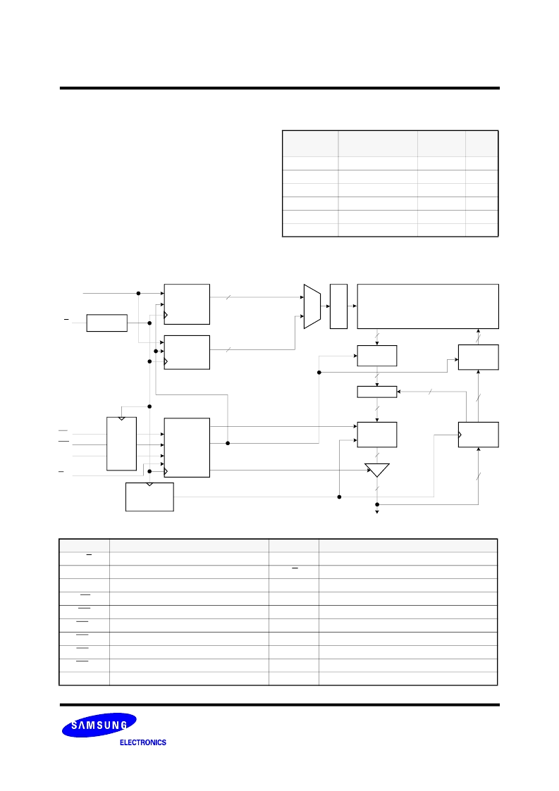
FUNCTIONAL BLOCK DIAGRAM
17 or 18
K,K
SS
SW
ZZ
G
Memory Array
128Kx36
256Kx18
Data Out
Data In
S/A Array
MUX0
W/D
Array
36 or 18
36 or 18
36 or 18
36 or 18
2:1
MUX
Dec.
SA[0:16]
or [0:17]
Address
Register
Read
Internal
Clock
Generator
Write
Address
Register
Data Out
Register
Clock
Buffer
Control
Register
DQ
36 or 18
36 or 18
36 or 18
36 or 18
XDIN
Data In
Register
(2 stage)
17 or 18
Control
Logic
E
WAY
OE
36 or 18
Organization
Part Number
Maximum
Frequency
Access
Time
128Kx36
K7P403622B-HC25
250MHz
2.5
128Kx36
K7P403622B-HC20
200MHz
2.7
128Kx36
K7P403622B-HC16
166MHz
3.0
256Kx18
K7P401822B-HC25
250MHz
2.5
256Kx18
K7P401822B-HC20
200MHz
2.7
256Kx18
K7P401822B-HC16
166MHz
3.0
相關(guān)PDF資料 |
PDF描述 |
|---|---|
| K7P403622B | 128Kx36 & 256Kx18 Synchronous Pipelined SRAM |
| K7P403622B-HC16 | 128Kx36 & 256Kx18 Synchronous Pipelined SRAM |
| K7Q161852A | 512Kx36 & 1Mx18 QDRTM b2 SRAM |
| K7Q163652A | Electrical Outlet Connector; Voltage Rating:125V; Contact Plating:Nickel; Current Rating:30A RoHS Compliant: Yes |
| K7Q161854A | 512Kx36-bit, 1Mx18-bit QDR SRAM |
相關(guān)代理商/技術(shù)參數(shù) |
參數(shù)描述 |
|---|---|
| K7P403622M | 制造商:SAMSUNG 制造商全稱:Samsung semiconductor 功能描述:128Kx36 & 256Kx18 Synchronous Pipelined SRAM |
| K7P403622M-H16 | 制造商:SAMSUNG 制造商全稱:Samsung semiconductor 功能描述:128Kx36 & 256Kx18 Synchronous Pipelined SRAM |
| K7P403622M-H19 | 制造商:SAMSUNG 制造商全稱:Samsung semiconductor 功能描述:128Kx36 & 256Kx18 Synchronous Pipelined SRAM |
| K7P403622M-H20 | 制造商:SAMSUNG 制造商全稱:Samsung semiconductor 功能描述:128Kx36 & 256Kx18 Synchronous Pipelined SRAM |
| K7P403622M-HC16000 | 制造商:Samsung SDI 功能描述: |
發(fā)布緊急采購,3分鐘左右您將得到回復(fù)。