- 您現在的位置:買賣IC網 > PDF目錄374294 > K7Q163682A (SAMSUNG SEMICONDUCTOR CO. LTD.) 512Kx36 & 1Mx18 QDR b2 SRAM PDF資料下載
參數資料
| 型號: | K7Q163682A |
| 廠商: | SAMSUNG SEMICONDUCTOR CO. LTD. |
| 英文描述: | 512Kx36 & 1Mx18 QDR b2 SRAM |
| 中文描述: | 512Kx36 |
| 文件頁數: | 10/17頁 |
| 文件大小: | 503K |
| 代理商: | K7Q163682A |
512Kx36 & 1Mx18 QDR
TM
b2 SRAM
- 10 -
Rev 1.0
July 2002
K7Q163682A
K7Q161882A
AC TIMING CHARACTERISTICS
(V
DD
=1.8V
±
0.1V, T
A
=0
°
C to +70
°
C)
Notes
: 1. All address inputs must meet the specified setup and hold times for all latching clock edges.
2. Control signales are R, W,BW
0
,BW
1
and (BW
2
, BW
3
, also for x36)
3. If C,C are tied high, K,K become the references for C,C timing parameters.
4. To avoid bus contention, at a given voltage and temperature tCHQX
1
is bigger than tCHQZ.
The specs as shown do not imply bus contention beacuse tCHQX
1
is a MIN parameter that is worst case at totally different test conditions
(0
°
C, 1.9V) than tCHQZ, which is a MAX parameter(worst case at 70
°
C, 1.7V)
It is not possible for two SRAMs on the same board to be at such different voltage and temperature.
PARAMETER
SYMBOL
-15
-13
-10
UNITS
NOTES
MIN
MAX
MIN
MAX
MIN
MAX
Clock
Clock Cycle Time(K, K, C, C)
t
KHKH
6.7
7.5
10
ns
Clock HIGH time (K, K, C, C)
t
KHKL
2.7
3.0
3.5
ns
Clock LOW time (K, K, C, C)
t
KLKH
2.7
3.0
3.5
ns
Clock to clock (K
↑ →
K
↑
, C
↑
→
C
↑
)
Clock to data clock (K
↑ →
C
↑
, K
↑→
C
↑
)
t
KHKH
3.0
3.7
3.4
4.1
4.6
5.4
ns
t
KHCH
0.0
2.2
0.0
2.5
0.0
3.0
ns
Output Times
C, C High to Output Valid
t
CHQV
2.7
3.0
3.0
ns
3
C, C High to Output Hold
t
CHQX
1.2
1.2
1.2
ns
3
C High to Output High-Z
t
CHQZ
2.7
3.0
3.0
ns
3
C High to Output Low-Z
t
CHQX1
1.2
1.2
1.2
ns
3
Setup Times
Address valic to K rising edge
t
AVKH
0.7
0.8
1.0
ns
Control inputs valid to K rising edge
t
IVKH
0.7
0.8
1.0
ns
2
Data-in varid to K, K rising edge
t
DVKH
0.7
0.8
1.0
ns
Hold Times
K rising edge to address hold
t
KHAX
0.7
0.8
1.0
v
K rising edge to control inputs hold
t
KHIX
0.7
0.8
1.0
ns
K, K rising edge to data-in hold
t
KHDX
0.7
0.8
1.0
ns
OPERATING CONDITIONS
(0
°
C
≤
T
A
≤
70
°
C)
PARAMETER
SYMBOL
MIN
MAX
UNIT
Supply Voltage
V
DD
1.7
1.9
V
V
DDQ
1.4
1.9
V
Reference
Voltage
Ground
V
REF
0.68
0.95
V
V
SS
0
0
V
Note:
For power-up, V
IH
≤
V
DDQ
+0.3V and V
DD
≤
1.7V and V
DDQ
≤
1.4V for t
≤
200ms
V
DDQ
V
IL
V
DDQ
+0.5V
20% t
KHKH
(MIN)
V
SS
V
IH
V
SS
-0.5V
20% t
KHKH
(MIN)
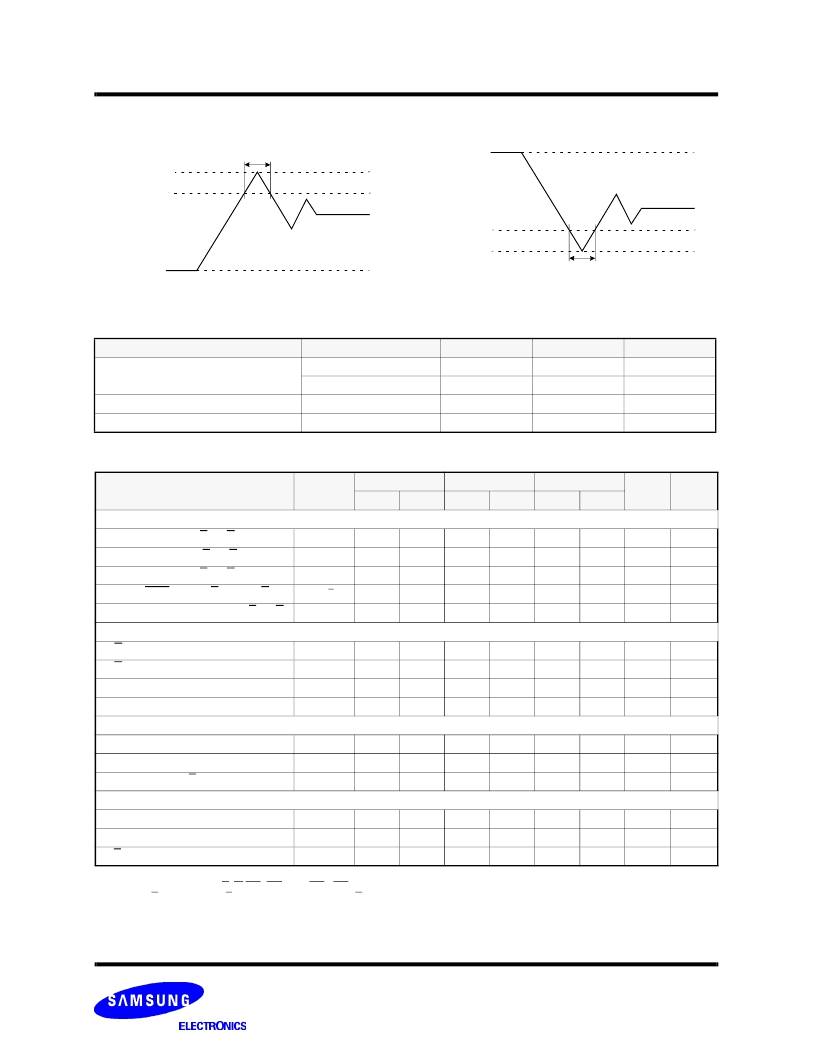
Undershoot Timing
Overershoot Timing
相關PDF資料 |
PDF描述 |
|---|---|
| K7R160982B | 512Kx36 & 1Mx18 & 2Mx9 QDRTM II b2 SRAM |
| K7R161882B | 512Kx36 & 1Mx18 & 2Mx9 QDRTM II b2 SRAM |
| K7R163682B | 512Kx36 & 1Mx18 & 2Mx9 QDRTM II b2 SRAM |
| K7R321884M-FC16 | 1Mx36 & 2Mx18 QDRTM II b4 SRAM |
| K7R323684M | 1Mx36 & 2Mx18 QDRTM II b4 SRAM |
相關代理商/技術參數 |
參數描述 |
|---|---|
| K7Q801854C-FC16000 | 制造商:Samsung Semiconductor 功能描述:8MSYNCQUAD DATA RATE SRAMEX18FBGA - Bulk |
| K7Q801854C-FC16T00 | 制造商:Samsung Semiconductor 功能描述:8MSYNCQUAD DATA RATE SRAMEX18FBGA, T/R - Tape and Reel |
| K7R160982B | 制造商:SAMSUNG 制造商全稱:Samsung semiconductor 功能描述:512Kx36 & 1Mx18 & 2Mx9 QDRTM II b2 SRAM |
| K7R161882B | 制造商:SAMSUNG 制造商全稱:Samsung semiconductor 功能描述:512Kx36 & 1Mx18 & 2Mx9 QDRTM II b2 SRAM |
| K7R161884B | 制造商:SAMSUNG 制造商全稱:Samsung semiconductor 功能描述:512Kx36 & 1Mx18 QDRTM II b4 SRAM |
發(fā)布緊急采購,3分鐘左右您將得到回復。