- 您現在的位置:買賣IC網 > PDF目錄374296 > K9F1608W0A-TIB0 (SAMSUNG SEMICONDUCTOR CO. LTD.) TV 37C 37#16 PIN RECP PDF資料下載
參數資料
| 型號: | K9F1608W0A-TIB0 |
| 廠商: | SAMSUNG SEMICONDUCTOR CO. LTD. |
| 英文描述: | TV 37C 37#16 PIN RECP |
| 中文描述: | 200萬× 8位NAND閃存 |
| 文件頁數: | 2/25頁 |
| 文件大?。?/td> | 443K |
| 代理商: | K9F1608W0A-TIB0 |
K9F1608W0A-TCB0, K9F1608W0A-TIB0
FLASH MEMORY
2
2M x 8 Bit NAND Flash Memory
The K9F1608W0A is a 2M(2,097,152)x8bit NAND Flash Mem-
ory with a spare 64K(65,536)x8bit. Its NAND cell provides the
most cost-effective solution for the solid state mass storage
market. A program operation programs the 264-byte page in
typically 250
μ
s and an erase operation can be performed in typ-
ically 2ms on a 4K-byte block.
Data in the page can be read out at 80ns cycle time per byte.
The I/O pins serve as the ports for address and data input/out-
put as well as command inputs. The on-chip write controller
automates all program and erase system functions, including
pulse repetition, where required, and internal verify and margin-
ing of data. Even the write-intensive systems can take advan-
tage of the K9F1608W0A extended reliability of 1,000,000
program/erase cycles by providing either ECC(Error Correction
Code) or real time mapping-out algorithm. These algorithms
have been implemented in many mass storage applications and
also the spare 8bytes of a page combined with the other 256
bytes can be utilized by system-level ECC.
The K9F1608W0A is an optimum solution for large nonvolatile
storage application such as solid state storage, digital voice
recorder, digital still camera and other portable applications
requiring nonvolatility.
GENERAL DESCRIPTION
FEATURES
Voltage Supply : 2.7V ~ 5.5V
Organization
- Memory Cell Array : (2M + 64K)bit x 8bit
- Data Register : (256 + 8)bit x8bit
Automatic Program and Erase
- Page Program : (256 + 8)Byte
- Block Erase : (4K + 128)Byte
- Status Register
264-Byte Page Read Operation
- Random Access : 10
μ
s(Max.)
- Serial Page Access : 80ns(Min.)
Fast Write Cycle Time
- Program time : 250
μ
s(typ.)
- Block Erase time : 2ms (typ.)
Command/Address/Data Multiplexed I/O port
Hardware Data Protection
- Program/Erase Lockout During Power Transitions
Reliable CMOS Floating-Gate Technology
- Endurance : 1M Program/Erase Cycles
- Data Retention : 10 years
Command Register Operation
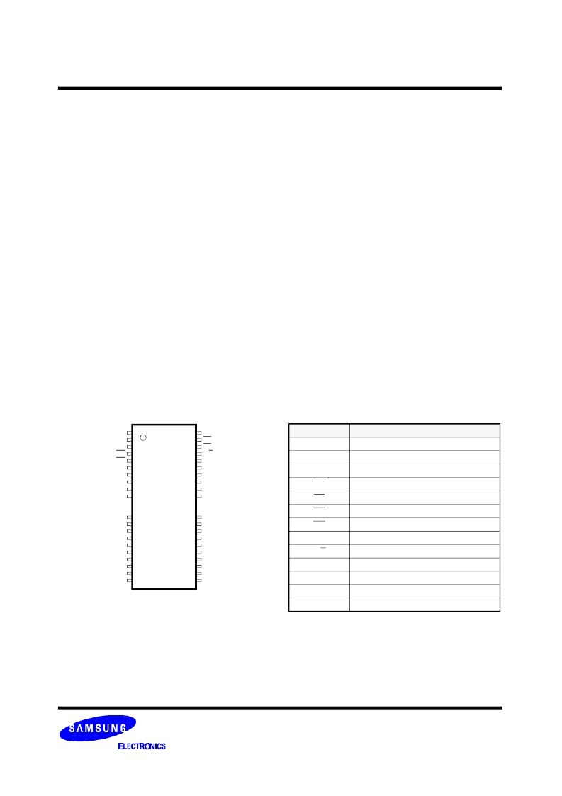
44(40) - Lead TSOP Type II (400mil / 0.8 mm pitch)
- Forward Type
PIN CONFIGURATION
V
SS
CLE
ALE
WE
WP
N.C
N.C
N.C
N.C
N.C
N.C
N.C
N.C
N.C
N.C
I/O0
I/O1
I/O2
I/O3
V
SS
1
2
3
4
5
6
7
8
9
10
11
12
13
14
15
16
17
18
19
20
21
22
V
CC
Q
I/O4
I/O5
I/O6
I/O7
N.C
N.C
N.C
N.C
N.C
N.C
N.C
N.C
N.C
N.C
GND
R/B
RE
CE
V
CC
23
24
25
26
27
28
29
30
31
32
33
34
35
36
37
38
39
40
41
42
43
44
44(40) TSOP (II)
STANDARD TYPE
NOTE
: Connect all V
CC
,VccQ
and V
SS
pins of each device to power supply outputs.
Do not leave V
CC
or V
SS
disconnected.
Pin Name
Pin Function
I/O0 ~ I/O7
Data Inputs/Outputs
CLE
Command Latch Enable
ALE
Address Latch Enable
CE
Chip Enable
RE
Read Enable
WE
Write Enable
WP
Write Protect
GND
Ground Input
R/B
Ready/Busy output
V
CC
Power(2.7V~5.5V)
V
CC
Q
Output Butter Power(2.7V~5.5V)
V
SS
Ground
N.C
No Connection
PIN DESCRIPTION
相關PDF資料 |
PDF描述 |
|---|---|
| K9F1G08Q0A | FLASH MEMORY |
| K9F1G08U0A | FLASH MEMORY |
| K9F1G08Q0M-YIB0 | 1Gb Gb 1.8V NAND Flash Errata |
| K9F1G16Q0M-YCB0 | 1Gb Gb 1.8V NAND Flash Errata |
| K9F1G08U0M-YCB0 | 1Gb Gb 1.8V NAND Flash Errata |
相關代理商/技術參數 |
參數描述 |
|---|---|
| K9F1G08B0C-PCB0T00 | 制造商:Samsung Semiconductor 功能描述:1GB SLC NORMAL X8 FBGA - Trays |
| K9F1G08D0M | 制造商:SAMSUNG 制造商全稱:Samsung semiconductor 功能描述:128M x 8 Bit / 64M x 16 Bit NAND Flash Memory |
| K9F1G08Q0A | 制造商:SAMSUNG 制造商全稱:Samsung semiconductor 功能描述:FLASH MEMORY |
| K9F1G08Q0M | 制造商:SAMSUNG 制造商全稱:Samsung semiconductor 功能描述:128M x 8 Bit / 64M x 16 Bit NAND Flash Memory |
| K9F1G08Q0M-PCB0 | 制造商:SAMSUNG 制造商全稱:Samsung semiconductor 功能描述:1Gb Gb 1.8V NAND Flash Errata |
發(fā)布緊急采購,3分鐘左右您將得到回復。