- 您現(xiàn)在的位置:買(mǎi)賣(mài)IC網(wǎng) > PDF目錄374304 > KA3524 (FAIRCHILD SEMICONDUCTOR CORP) SMPS Controller PDF資料下載
參數(shù)資料
| 型號(hào): | KA3524 |
| 廠商: | FAIRCHILD SEMICONDUCTOR CORP |
| 元件分類(lèi): | 穩(wěn)壓器 |
| 英文描述: | SMPS Controller |
| 中文描述: | 0.1 A SWITCHING CONTROLLER, 350 kHz SWITCHING FREQ-MAX, PDIP16 |
| 封裝: | DIP-16 |
| 文件頁(yè)數(shù): | 5/12頁(yè) |
| 文件大小: | 103K |
| 代理商: | KA3524 |
KA3524
5
Error Amplifier
This circuit is a simple differential-input, transconductance amplifier. The output is the compensation terminal pin 9, which is
a high impedance node (R
L:
=5M
). The gain is
G
V
= gmR
L
=
= 0.002 R
L
and can easily be reduced from a nominal of 10,000 by an external shunt resistance from pin 9 to ground, as shown in Figure
8,In addition to DC gain control, the compensation terminal is also the place for AC phase compensation. The frequency
response curves of Figure 5 show the uncompensated amplifier with a single pole at approximately 200Hz and a unity gain
cross-over frequency at 5MHz.typically, most output filter designs will introduce one or more addition poles at a significantly
higher power frequency. Therefore, the best stabilizing network is a series R-C combination between pin 9 and ground which
introduces a zero to cancel one of the output filter poles. A good starting point is 50K
plus 0.001 micro farad. One final point
on the compensation terminal is that this is also a convenient place to insert any programming signal which is to override the
error amplifier. Internal shutdown and current limit circuits are connected here, but any other circuit which can sink 200uA
can pull this point to ground, thus shutting off both outputs. While feedback is normally applied around the entire regulator, the
error amplifier can be used with conventional operational amplifier feedback and is stable in either the inverting or non-
inverting mode. Regardless of the connections, however, input common-mode limits must be observed or output sign inver-
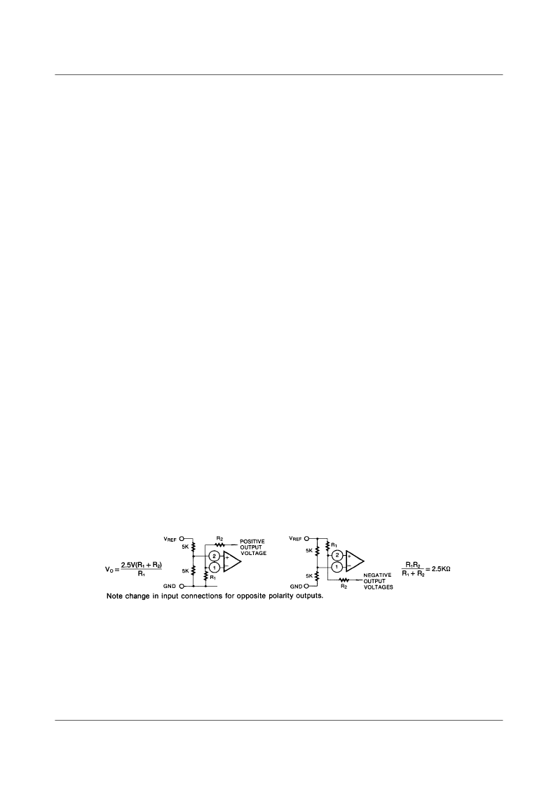
sions may happen. For conventional regulator applications, the 5 volt reference voltage must be divided down as shown in Fig-
ure 3. The error amplifier may also be used in fixed duty cycle applications by using the unity gain configuration shown in the
open loop test circuit.
Current Limiting
The current limiting circuitry of the KA3524 is shown in Figure 4.
By matching the base-emitter voltages of Q1 and Q2, and assuming negligible voltage drop across R
1
:
Threshold = V
BE
(Q1) + I
1
R
2
- V
BE
(Q2)
= l
1
R
2
= 200mV
Although this circuit provides a relatively small threshold with a negligible temperature coefficient, there are some limitations
to its use, the most important of which is the
±
1 volt common mode range which requires sensing in the ground line. Another
factor to consider is that the frequency compensation provided by R
1
C
1
and Q1 provides a roll-off pole at approximately
300Hz.Since the gain of this circuit is relatively low, there is a transition region as the current limit amplifier takes over pulse
width control from the error amplifier. For testing purposes, the threshold is defined as the input voltage to get 25% duty cycle
with the error amplifier signaling maximum duty cycle. In addition to constant current limiting, pins 4 and 5 may also be used
in transformer-coupled circuits to sense primary current and shorten an output pulse, should transformer saturation occur.
Another application is to ground pin 5 and use pin 4 as an additional shutdown terminal: i.e., the output will be off with pin 4
open and on when it is grounded. Finally, fold back current limiting can be provided with the network of Figure 5. This cir-
cuit can reduce the short circuit current (l
SC
)to approximately one third the maximum available output current (I
MAX
).
Figure 3. Error Amplifier Biasing Circuits
8I
R
L
2K
T
---------------
相關(guān)PDF資料 |
PDF描述 |
|---|---|
| KA3525A | SMPS CONTROLLER |
| KA3525AD | SMPS CONTROLLER |
| KA3842AE | SMPS Controller |
| KA3842 | Linear Integrated Circuit(CURRENT-MODE PWM CONTROLLER) |
| KA3842A | Linear Integrated Circuit(CURRENT-MODE PWM CONTROLLER) |
相關(guān)代理商/技術(shù)參數(shù) |
參數(shù)描述 |
|---|---|
| KA3525A | 功能描述:DC/DC 開(kāi)關(guān)控制器 SMPS Controller RoHS:否 制造商:Texas Instruments 輸入電壓:6 V to 100 V 開(kāi)關(guān)頻率: 輸出電壓:1.215 V to 80 V 輸出電流:3.5 A 輸出端數(shù)量:1 最大工作溫度:+ 125 C 安裝風(fēng)格: 封裝 / 箱體:CPAK |
| KA3525A | 制造商:Fairchild Semiconductor Corporation 功能描述:CONTROLLER IC 制造商:Fairchild Semiconductor Corporation 功能描述:IC, SMPS CONTROLLER, 16-DIP |
| KA3525AD | 制造商:FAIRCHILD 制造商全稱(chēng):Fairchild Semiconductor 功能描述:SMPS CONTROLLER |
| KA-3528 | 制造商:KINGBRIGHT 制造商全稱(chēng):Kingbright Corporation 功能描述:3.5 x 2.8mm SURFACE MOUNT LED LAMPS |
| KA-3528ACGCK | 制造商:Kingbright Corporation 功能描述: |
發(fā)布緊急采購(gòu),3分鐘左右您將得到回復(fù)。