- 您現(xiàn)在的位置:買賣IC網(wǎng) > PDF目錄374311 > KBE00G003M (SAMSUNG SEMICONDUCTOR CO. LTD.) NAND 512Mb*2 + Mobile SDRAM 256Mb*2 PDF資料下載
參數(shù)資料
| 型號: | KBE00G003M |
| 廠商: | SAMSUNG SEMICONDUCTOR CO. LTD. |
| 英文描述: | NAND 512Mb*2 + Mobile SDRAM 256Mb*2 |
| 中文描述: | NAND閃存的512Mb * 2移動SDRAM 256Mb的* 2 |
| 文件頁數(shù): | 20/89頁 |
| 文件大?。?/td> | 1238K |
| 代理商: | KBE00G003M |
第1頁第2頁第3頁第4頁第5頁第6頁第7頁第8頁第9頁第10頁第11頁第12頁第13頁第14頁第15頁第16頁第17頁第18頁第19頁當前第20頁第21頁第22頁第23頁第24頁第25頁第26頁第27頁第28頁第29頁第30頁第31頁第32頁第33頁第34頁第35頁第36頁第37頁第38頁第39頁第40頁第41頁第42頁第43頁第44頁第45頁第46頁第47頁第48頁第49頁第50頁第51頁第52頁第53頁第54頁第55頁第56頁第57頁第58頁第59頁第60頁第61頁第62頁第63頁第64頁第65頁第66頁第67頁第68頁第69頁第70頁第71頁第72頁第73頁第74頁第75頁第76頁第77頁第78頁第79頁第80頁第81頁第82頁第83頁第84頁第85頁第86頁第87頁第88頁第89頁
KBE00G003M-D411
MCP MEMORY
July 2005
20
Revision 0.1
Samsung NAND Flash has three address pointer commands as a substitute for the two most significant column addresses. ’00h’
command sets the pointer to ’A’ area(0~255byte), ’01h’ command sets the pointer to ’B’ area(256~511byte), and ’50h’ command sets
the pointer to ’C’ area(512~527byte). With these commands, the starting column address can be set to any of a whole
page(0~527byte). ’00h’ or ’50h’ is sustained until another address pointer command is inputted. ’01h’ command, however, is effective
only for one operation. After any operation of Read, Program, Erase, Reset, Power_Up is executed once with ’01h’ command, the
address pointer returns to ’A’ area by itself. To program data starting from ’A’ or ’C’ area, ’00h’ or ’50h’ command must be inputted
before ’80h’ command is written. A complete read operation prior to ’80h’ command is not necessary. To program data starting from
’B’ area, ’01h’ command must be inputted right before ’80h’ command is written.
00h
(1) Command input sequence for programming ’A’ area
Address / Data input
80h
10h
00h
80h
10h
Address / Data input
The address pointer is set to ’A’ area(0~255), and sustained
01h
(2) Command input sequence for programming ’B’ area
Address / Data input
80h
10h
01h
80h
10h
Address / Data input
’B’, ’C’ area can be programmed.
It depends on how many data are inputted.
’01h’ command must be rewritten before
every program operation
The address pointer is set to ’B’ area(256~511), and will be reset to
’A’ area after every program operation is executed.
50h
(3) Command input sequence for programming ’C’ area
Address / Data input
80h
10h
50h
80h
10h
Address / Data input
Only ’C’ area can be programmed.
’50h’ command can be omitted.
The address pointer is set to ’C’ area(512~527), and sustained
’00h’ command can be omitted.
It depends on how many data are inputted.
’A’,’B’,’C’ area can be programmed.
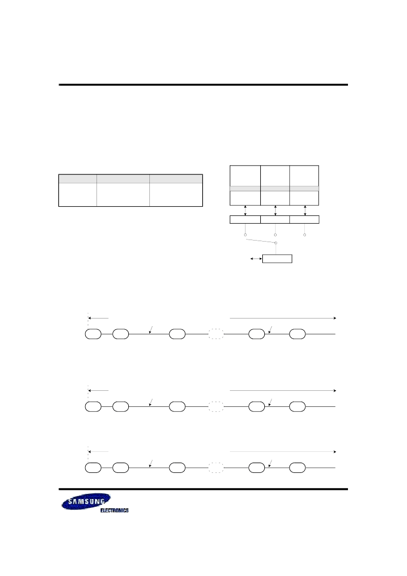
Pointer Operation
Table 2. Destination of the pointer
Command
Pointer position
Area
00h
01h
50h
0 ~ 255 byte
256 ~ 511 byte
512 ~ 527 byte
1st half array(A)
2nd half array(B)
spare array(C)
"A" area
(00h plane)
256 Byte
"B" area
(01h plane)
"C" area
(50h plane)
256 Byte
16 Byte
"A"
"B"
"C"
Internal
Page Register
Pointer select
commnad
(00h, 01h, 50h)
Pointer
Figure 5. Block Diagram of Pointer Operation
相關(guān)PDF資料 |
PDF描述 |
|---|---|
| KBE00G003M-D411 | NAND 512Mb*2 + Mobile SDRAM 256Mb*2 |
| KBE00S009M | 1Gb NAND x 2 + 256Mb Mobile SDRAM x 2 |
| KBE00S009M-D411 | 1Gb NAND x 2 + 256Mb Mobile SDRAM x 2 |
| KBJ2501 | 25A SINGLE PHASE SILICON BRIDGE RECTIFIER |
| KBJ2502 | 25A SINGLE PHASE SILICON BRIDGE RECTIFIER |
相關(guān)代理商/技術(shù)參數(shù) |
參數(shù)描述 |
|---|---|
| KBE00G003M-D411 | 制造商:SAMSUNG 制造商全稱:Samsung semiconductor 功能描述:NAND 512Mb*2 + Mobile SDRAM 256Mb*2 |
| KBE00S003M | 制造商:SAMSUNG 制造商全稱:Samsung semiconductor 功能描述:1Gb NAND*2 + 256Mb Mobile SDRAM*2 |
| KBE00S003M-D411 | 制造商:SAMSUNG 制造商全稱:Samsung semiconductor 功能描述:1Gb NAND*2 + 256Mb Mobile SDRAM*2 |
| KBE00S009M | 制造商:SAMSUNG 制造商全稱:Samsung semiconductor 功能描述:1Gb NAND x 2 + 256Mb Mobile SDRAM x 2 |
| KBE00S009M-D411 | 制造商:SAMSUNG 制造商全稱:Samsung semiconductor 功能描述:1Gb NAND x 2 + 256Mb Mobile SDRAM x 2 |
發(fā)布緊急采購,3分鐘左右您將得到回復。