- 您現(xiàn)在的位置:買賣IC網(wǎng) > PDF目錄374332 > KFM1216Q2M-DED (SAMSUNG SEMICONDUCTOR CO. LTD.) FLASH MEMORY PDF資料下載
參數(shù)資料
| 型號: | KFM1216Q2M-DED |
| 廠商: | SAMSUNG SEMICONDUCTOR CO. LTD. |
| 英文描述: | FLASH MEMORY |
| 中文描述: | 閃存 |
| 文件頁數(shù): | 52/88頁 |
| 文件大小: | 1150K |
| 代理商: | KFM1216Q2M-DED |
第1頁第2頁第3頁第4頁第5頁第6頁第7頁第8頁第9頁第10頁第11頁第12頁第13頁第14頁第15頁第16頁第17頁第18頁第19頁第20頁第21頁第22頁第23頁第24頁第25頁第26頁第27頁第28頁第29頁第30頁第31頁第32頁第33頁第34頁第35頁第36頁第37頁第38頁第39頁第40頁第41頁第42頁第43頁第44頁第45頁第46頁第47頁第48頁第49頁第50頁第51頁當(dāng)前第52頁第53頁第54頁第55頁第56頁第57頁第58頁第59頁第60頁第61頁第62頁第63頁第64頁第65頁第66頁第67頁第68頁第69頁第70頁第71頁第72頁第73頁第74頁第75頁第76頁第77頁第78頁第79頁第80頁第81頁第82頁第83頁第84頁第85頁第86頁第87頁第88頁
MuxOneNAND512(KFM1216Q2M)
FLASH MEMORY
52
8.6 Read Operation
The device has two read configurations ; Asynchronous read and Synchronous burst read.
The initial state machine makes the device to be automatically entered into asynchronous read mode to prevent the memory content
from spurious altering upon device power up or after a hardware reset. No commands are required to retrieve data in asynchronous
mode. The synchronous mode will be enabled by setting RM bit of System configuration1 register to Synchronous read mode.
8.6.1 Asynchronous Read Mode (RM = 0)
For the asynchronous read mode a valid address should be asserted on ADQ0-ADQ15, while driving AVD and CE to V
IL
. WE
should remain at V
IH
. The data will appear on ADQ15-ADQ0. Address access time (t
AA
) is equal to the delay from valid addresses to
valid output data. The chip enable access time(t
CE
) is the delay from the falling edge of CE to valid data at the outputs. The output
enable access time(t
OE
) is the delay from the falling edge of OE to valid data at the output.
8.6.2 Synchronous (Burst) Read Mode (RM = 1)
The device is capable of continuous linear burst operation and linear burst operation of a preset length. For the burst mode, the host
should determine how many clock cycles are desired for the initial word(t
IAA
) of each burst access using BRL bit of System configura-
tion 1 register. The registers also can be read during burst read mode by using AVD signal with a address. To initiate the synchro-
nous read again, a new address during CE low and AVD toggle is needed after the host has completed status reads or the device has
completed the program or erase operation.
8.6.3 Continuous Linear Burst Read
The initial word is output t
IAA
after the rising edge of the first CLK cycle. Subsequent words are output t
BA
after the rising edge of each
successive clock cycle, which automatically increments the internal address counter. The RDY output indicates this condition to the
system by pulsing low. The device will continue to output sequential burst data, wrapping around after it reaches the designated loca-
tion(See Figure 12 for address map information) until the system asserts CE high, RP low or AVD low in conjunction with a new
address. The cold/warm/hot reset or asserting CE high or WE low pulse terminate the burst read operation.
If the device is accessed synchronously while it is set to asynchronous read mode, it is possible to read out the first data without prob-
lems.
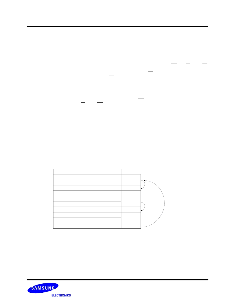
Division
Add.map(word order)
BootM(0.5Kw)
0000h~01FFh
Buffer0
BufM 0(1Kw)
0200h~05FFh
BufM 1(1Kw)
0600h~09FFh
Buffer1
Reserved Main
0A00h~7FFFh
N/A Reg.
BootS(16w)
8000H~800Fh
Buffer0
BufS 0(32w)
8010h~802Fh
BufS 1(32w)
8030h~804Fh
Buffer1
Reserved Spare
8050h~8FFFh
N/A Reg.
Reserved Reg.
9000h~EFFFh
Register(4Kw)
F000h~FFFFh
Reg.
Not Support
Not Support
Not Support
Figure 12. The boundary of synchronous read
* Reserved area is not available on Synchronous read
相關(guān)PDF資料 |
PDF描述 |
|---|---|
| KFM210M | SPECIFICATIONS FOR SAW FILTER(BAND PASS FILTERS FOR US PCS IF STAGE) |
| KFM220M | SPECIFICATIONS FOR SAW FILTER(BAND PASS FILTERS FOR KOREAN PCS IF STAGE) |
| KFM85M | SPECIFICATIONS FOR SAW FILTER(BAND PASS FILTERS FOR CDMA IF STAGE) |
| KFN2G16Q2M-DEB5 | MuxOneNAND FLASH MEMORY |
| KFM1G16Q2M | MuxOneNAND FLASH MEMORY |
相關(guān)代理商/技術(shù)參數(shù) |
參數(shù)描述 |
|---|---|
| KFM17113 | 制造商:Luxo 功能描述:KFM ILLUMINATED MAGNIFIER W/CLAMP 3-DIOPTER 45" BLAC |
| KFM1G16Q2B-DEB8000 | 制造商:Samsung Semiconductor 功能描述:1GB ONENAND X16 FBGA - Trays |
| KFM1G16Q2M | 制造商:SAMSUNG 制造商全稱:Samsung semiconductor 功能描述:MuxOneNAND FLASH MEMORY |
| KFM1G16Q2M-DEB5 | 制造商:SAMSUNG 制造商全稱:Samsung semiconductor 功能描述:MuxOneNAND FLASH MEMORY |
| KFM1G16Q2M-DEB6 | 制造商:SAMSUNG 制造商全稱:Samsung semiconductor 功能描述:MuxOneNAND FLASH MEMORY |
發(fā)布緊急采購,3分鐘左右您將得到回復(fù)。