- 您現(xiàn)在的位置:買(mǎi)賣(mài)IC網(wǎng) > PDF目錄374354 > KM416RD4C (SAMSUNG SEMICONDUCTOR CO. LTD.) Direct Rambus DRAM(Direct Rambus 動(dòng)態(tài)RAM) PDF資料下載
參數(shù)資料
| 型號(hào): | KM416RD4C |
| 廠商: | SAMSUNG SEMICONDUCTOR CO. LTD. |
| 英文描述: | Direct Rambus DRAM(Direct Rambus 動(dòng)態(tài)RAM) |
| 中文描述: | 直接Rambus公司的DRAM(動(dòng)態(tài)內(nèi)存直接Rambus公司) |
| 文件頁(yè)數(shù): | 3/59頁(yè) |
| 文件大小: | 4654K |
| 代理商: | KM416RD4C |
第1頁(yè)第2頁(yè)當(dāng)前第3頁(yè)第4頁(yè)第5頁(yè)第6頁(yè)第7頁(yè)第8頁(yè)第9頁(yè)第10頁(yè)第11頁(yè)第12頁(yè)第13頁(yè)第14頁(yè)第15頁(yè)第16頁(yè)第17頁(yè)第18頁(yè)第19頁(yè)第20頁(yè)第21頁(yè)第22頁(yè)第23頁(yè)第24頁(yè)第25頁(yè)第26頁(yè)第27頁(yè)第28頁(yè)第29頁(yè)第30頁(yè)第31頁(yè)第32頁(yè)第33頁(yè)第34頁(yè)第35頁(yè)第36頁(yè)第37頁(yè)第38頁(yè)第39頁(yè)第40頁(yè)第41頁(yè)第42頁(yè)第43頁(yè)第44頁(yè)第45頁(yè)第46頁(yè)第47頁(yè)第48頁(yè)第49頁(yè)第50頁(yè)第51頁(yè)第52頁(yè)第53頁(yè)第54頁(yè)第55頁(yè)第56頁(yè)第57頁(yè)第58頁(yè)第59頁(yè)
Page 4
KM416RD4C/KM418RD4C
Direct RDRAM
Revision 0.7 September 1998
TARGET
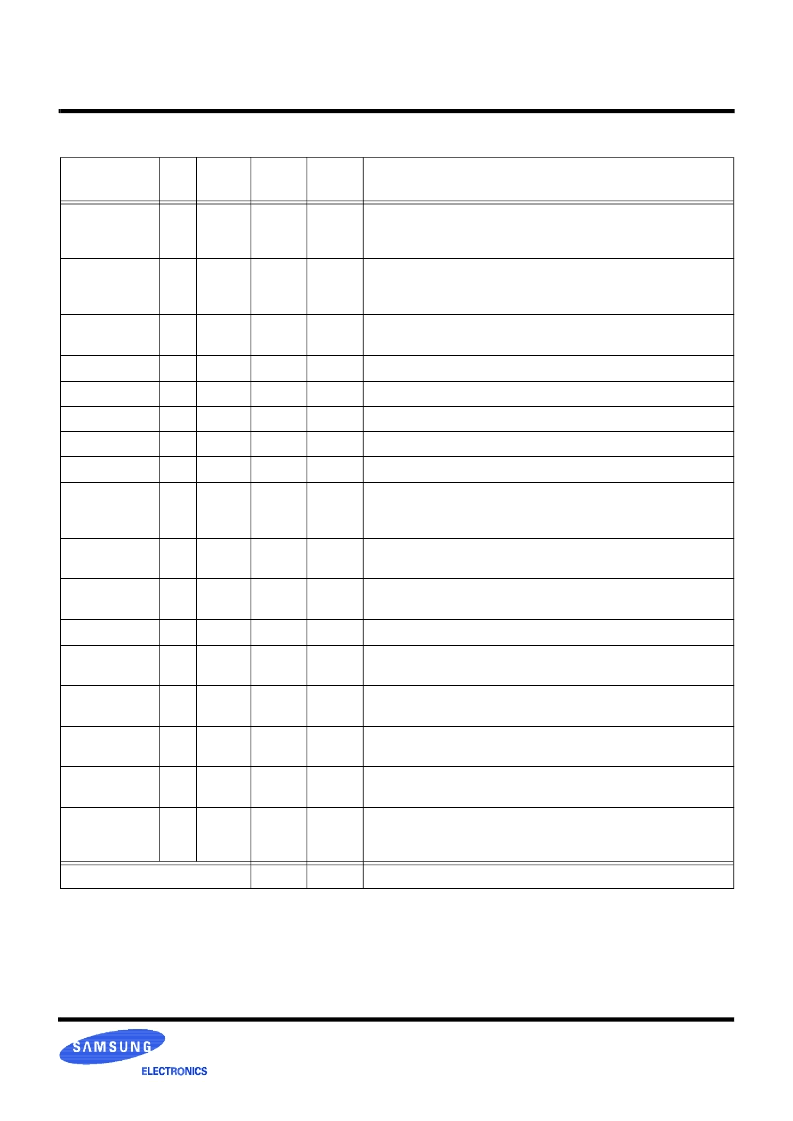
Table 3 : Pin Description
Signal
I/O
Type
# Pins
edge
# Pins
center
Description
SIO1,SIO0
I/O
CMOS
2
2
Serial input/output. Pins for reading from and writing to the control
registers using a serial access protocol. Also used for power man-
agement.
CMD
I
CMOS
1
1
Command input. Pins used in conjunction with SIO0 and SIO1 for
reading from and writing to the control registers. Also used for
power management.
SCK
I
CMOS
1
1
Serial clock input. Clock source used for reading from and writing
to the control registers
V
DD
14
6
Supply voltage for the RDRAM core and interface logic.
V
DDa
2
1
Supply voltage for the RDRAM analog circuitry.
V
CMOS
2
2
Supply voltage for CMOS input/output pins.
GND
19
9
Ground reference for RDRAM core and interface.
GNDa
2
1
Ground reference for RDRAM analog circuitry.
DQA8..DQA0
I/O
RSL
9
9
Data byte A. Nine pins which carry a byte of read or write data
between the Channel and the RDRAM. DQA8 is not used by
RDRAMs with a x16 organization.
CFM
I
RSL
1
1
Clock from master. Interface clock used for receiving RSL signals
from the Channel. Positive polarity.
CFMN
I
RSL
1
1
Clock from master. Interface clock used for receiving RSL signals
from the Channel. Negative polarity
V
REF
1
1
Logic threshold reference voltage for RSL signals
CTMN
I
RSL
1
1
Clock to master. Interface clock used for transmitting RSL signals
to the Channel. Negative polarity.
CTM
I
RSL
1
1
Clock to master. Interface clock used for transmitting RSL signals
to the Channel. Positive polarity.
RQ7..RQ5 or
ROW2..ROW0
I
RSL
3
3
Row access control. Three pins containing control and address
information for row accesses.
RQ4..RQ0 or
COL4..COL0
I
RSL
5
5
Column access control. Five pins containing control and address
information for column accesses.
DQB8..
DQB0
I/O
RSL
9
9
Data byte B. Nine pins which carry a byte of read or write data
between the Channel and the RDRAM. DQB8 is not used by
RDRAMs with a x16 organization.
Total pin count per package
74
54
相關(guān)PDF資料 |
PDF描述 |
|---|---|
| KM416S1021CT-G7 | 512K x 16Bit x 2 Banks Synchronous DRAM with SSTL interface |
| KM416S1021CT-G8 | 512K x 16Bit x 2 Banks Synchronous DRAM with SSTL interface |
| KM416S1021CT-GS | 512K x 16Bit x 2 Banks Synchronous DRAM with SSTL interface |
| KM416S1120D | 512K x 16bit x 2 Banks Synchronous DRAM LVTTL |
| KM416S16230A | 4M x 16Bit x 4 Banks Synchronous DRAM(4M x 16位 x4組同步動(dòng)態(tài)RAM) |
相關(guān)代理商/技術(shù)參數(shù) |
參數(shù)描述 |
|---|---|
| KM416RD4D | 制造商:SAMSUNG 制造商全稱(chēng):Samsung semiconductor 功能描述:128/144Mbit RDRAM 256K x 16/18 bit x 2*16 Dependent Banks Direct RDRAMTM |
| KM416RD8AC | 制造商:SAMSUNG 制造商全稱(chēng):Samsung semiconductor 功能描述:128/144Mbit RDRAM 256K x 16/18 bit x 2*16 Dependent Banks Direct RDRAMTM |
| KM416RD8AC(D)-RK70 | 制造商:SAMSUNG 制造商全稱(chēng):Samsung semiconductor 功能描述:128/144Mbit RDRAM 256K x 16/18 bit x 2*16 Dependent Banks Direct RDRAMTM |
| KM416RD8AC(D)-RK80 | 制造商:SAMSUNG 制造商全稱(chēng):Samsung semiconductor 功能描述:128/144Mbit RDRAM 256K x 16/18 bit x 2*16 Dependent Banks Direct RDRAMTM |
| KM416RD8AC(DB)-RCG60 | 制造商:SAMSUNG 制造商全稱(chēng):Samsung semiconductor 功能描述:128/144Mbit RDRAM 256K x 16/18 bit x 2*16 Dependent Banks Direct RDRAMTM |
發(fā)布緊急采購(gòu),3分鐘左右您將得到回復(fù)。