- 您現(xiàn)在的位置:買賣IC網(wǎng) > PDF目錄374356 > KM6164002B (SAMSUNG SEMICONDUCTOR CO. LTD.) 256K x 16 Bit High-Speed CMOS Static RAM(256Kx16位低功耗CMOS 靜態(tài) RAM) PDF資料下載
參數(shù)資料
| 型號(hào): | KM6164002B |
| 廠商: | SAMSUNG SEMICONDUCTOR CO. LTD. |
| 英文描述: | 256K x 16 Bit High-Speed CMOS Static RAM(256Kx16位低功耗CMOS 靜態(tài) RAM) |
| 中文描述: | 256K × 16位高速CMOS靜態(tài)RAM(256Kx16位低功耗的CMOS靜態(tài)RAM)的 |
| 文件頁(yè)數(shù): | 2/9頁(yè) |
| 文件大小: | 150K |
| 代理商: | KM6164002B |
KM6164002B, KM6164002BI
CMOS SRAM
PRELIMPreliminaryPPPPPPPPPINARY
Rev 2.1
June 1998
- 2 -
PRELIMINARY
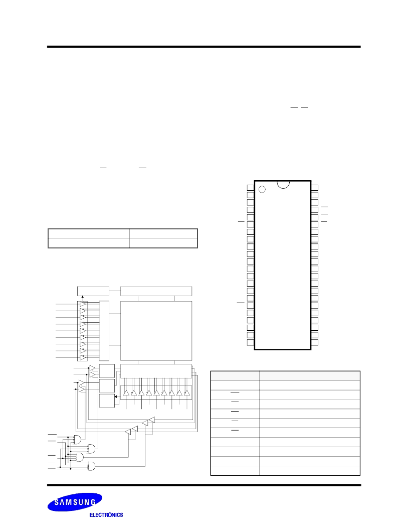
PIN FUNCTION
Pin Name
Pin Function
A
0
- A
17
Address Inputs
WE
Write Enable
CS
Chip Select
OE
Output Enable
LB
Lower-byte Control(I/O
1
~I/O
8
)
UB
Upper-byte Control(I/O
9
~I/O
16
)
I/O
1
~ I/O
16
Data Inputs/Outputs
V
CC
Power(+5.0V)
V
SS
Ground
N.C
No Connection
256K x 16 Bit High-Speed CMOS Static RAM
FEATURES
Fast Access Time 10,12,15ns(Max.)
Low Power Dissipation
Standby (TTL) : 50mA(Max.)
(CMOS) : 10mA(Max.)
Operating KM6164002B - 10 : 260mA(Max.)
KM6164002B - 12 : 255mA(Max.)
KM6164002B - 15 : 250mA(Max.)
Single 5.0V
±
10% Power Supply
TTL Compatible Inputs and Outputs
I/O Compatible with 3.3V Device
Fully Static Operation
- No Clock or Refresh required
Three State Outputs
Center Power/Ground Pin Configuration
Data Byte Control : LB : I/O
1
~ I/O
8,
UB : I/O
9
~ I/O
16
Standard Pin Configuration
KM6164002BJ : 44-SOJ-400
KM6164002BT : 44-TSOP2-400F
The KM6164002B is a 4,194,304-bit high-speed Static Random
Access Memory organized as 262,144 words by 16 bits. The
KM6164002B uses 16 common input and output lines and has
an output enable pin which operates faster than address
access time at read cycle. Also it allows that lower and upper
byte access by data byte control(UB, LB). The device is fabri-
cated using SAMSUNG
′
s advanced CMOS process and
designed for high-speed circuit technology. It is particularly well
suited for use in high-density high-speed system applications.
The KM6164002B is packaged in a 400mil 44-pin plastic SOJ
or TSOP(II) forward.
GENERAL DESCRIPTION
Clk Gen.
I/O
1
~I/O
8
OE
UB
LB
CS
PIN CONFIGURATION
(Top View)
SOJ/
TSOP2
FUNCTIONAL BLOCK DIAGRAM
R
Data
Cont.
Data
Cont.
Column Select
CLK
Gen.
Pre-Charge Circuit
Memory Array
512 Rows
512x16 Columns
I/O Circuit &
1
2
3
4
5
6
7
8
9
10
11
12
13
14
15
16
17
18
19
20
21
22
A
17
A
16
A
15
OE
UB
LB
I/O
16
I/O
15
I/O
14
I/O
13
Vss
Vcc
I/O
12
I/O
11
I/O
10
I/O
9
N.C
A
14
A
13
A
12
A
11
A
10
A
0
A
1
A
2
A
3
A
4
CS
I/O
1
I/O
2
I/O
3
I/O
4
Vcc
Vss
I/O
5
I/O
6
I/O
7
I/O
8
WE
A
5
A
6
A
7
A
8
A
9
I/O
9
~I/O
16
WE
44
43
42
41
40
39
38
37
36
35
34
33
32
31
30
29
28
27
26
25
24
23
A
10
A
12
A
14
A
16
A
9
A
11
A
13
A
15
A
17
KM6164002B -10/12/15
Commercial Temp.
KM6164002BI -10/12/15
Industrial Temp.
ORDERING INFORMATION
A
0
A
1
A
2
A
3
A
4
A
5
A
6
A
7
A
8
相關(guān)PDF資料 |
PDF描述 |
|---|---|
| KM6164002BI | 256K x 16 Bit High-Speed CMOS Static RAM(256Kx16位低功耗CMOS 靜態(tài) RAM) |
| KM6164002 | CMOS SRAM |
| KM6164002E | CMOS SRAM |
| KM6164002I | RES 0-OHM-JUMPER THK-FILM SMD-0402 TR-7-PA |
| KM616FR4110 | 256K x 16 Bit Super Low Power and Low Voltage Full CMOS Static RAM(256K x 16位超低功耗低電壓CMOS 靜態(tài)RAM) |
相關(guān)代理商/技術(shù)參數(shù) |
參數(shù)描述 |
|---|---|
| KM6164002E | 制造商:SAMSUNG 制造商全稱:Samsung semiconductor 功能描述:CMOS SRAM |
| KM6164002I | 制造商:SAMSUNG 制造商全稱:Samsung semiconductor 功能描述:CMOS SRAM |
| KM6164002J-20 FAB | 制造商:Samsung Semiconductor 功能描述: |
| KM616B4002J-12 | 制造商:SEC 功能描述: |
| KM6-16S-10PN | 制造商:Amphenol Corporation 功能描述:KM AUSTRALIAN PRODUCT - Bulk |
發(fā)布緊急采購(gòu),3分鐘左右您將得到回復(fù)。