- 您現(xiàn)在的位置:買賣IC網(wǎng) > PDF目錄374356 > KM6164002B (SAMSUNG SEMICONDUCTOR CO. LTD.) 256K x 16 Bit High-Speed CMOS Static RAM(256Kx16位低功耗CMOS 靜態(tài) RAM) PDF資料下載
參數(shù)資料
| 型號(hào): | KM6164002B |
| 廠商: | SAMSUNG SEMICONDUCTOR CO. LTD. |
| 英文描述: | 256K x 16 Bit High-Speed CMOS Static RAM(256Kx16位低功耗CMOS 靜態(tài) RAM) |
| 中文描述: | 256K × 16位高速CMOS靜態(tài)RAM(256Kx16位低功耗的CMOS靜態(tài)RAM)的 |
| 文件頁數(shù): | 3/9頁 |
| 文件大小: | 150K |
| 代理商: | KM6164002B |
KM6164002B, KM6164002BI
CMOS SRAM
PRELIMPreliminaryPPPPPPPPPINARY
Rev 2.1
June 1998
- 3 -
PRELIMINARY
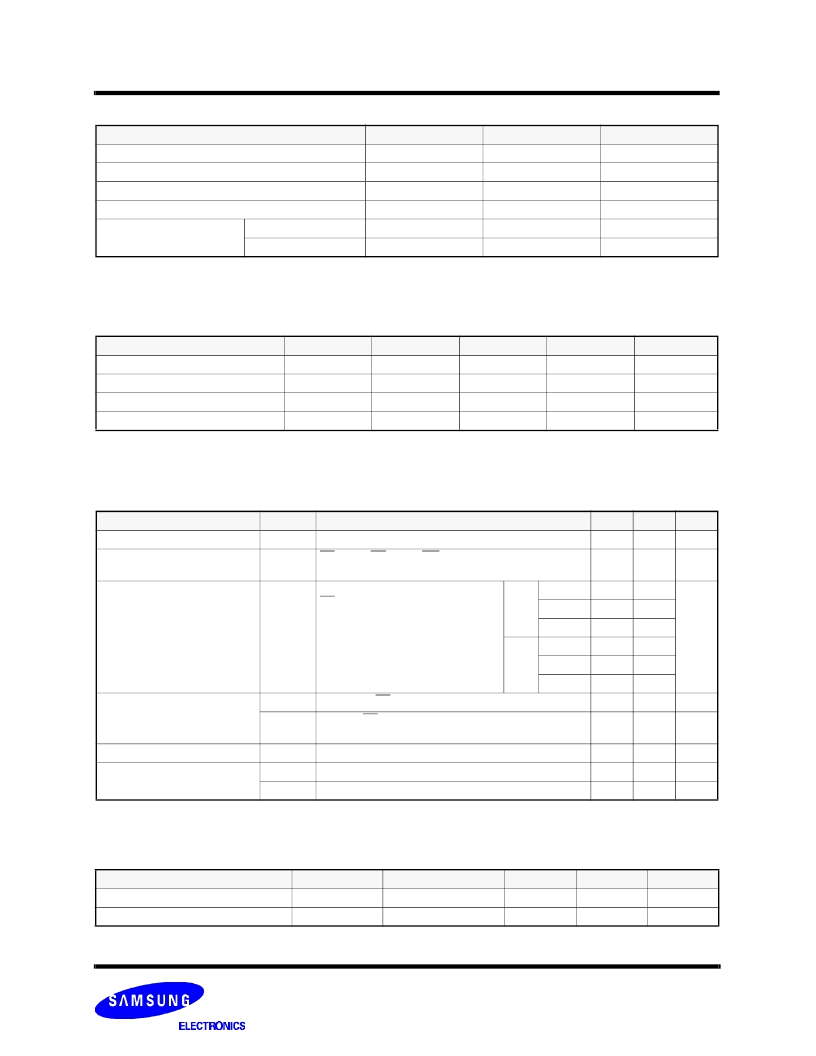
DC AND OPERATING CHARACTERISTICS
(T
A
=0 to 70
°
C, Vcc= 5.0V
±
10%, unless otherwise specified)
NOTE: The above parameters are also guaranteed at industrial temperature range.
* V
CC
=5.0V
,
Temp.=25
°
C
Parameter
Symbol
Test Conditions
Min
Max
Unit
Input Leakage Current
I
LI
V
IN
=V
SS
to
V
CC
-2
2
μ
A
μ
A
Output Leakage Current
I
LO
CS=V
IH
or OE=V
IH
or WE=V
IL
V
OUT
= V
SS
to
V
CC
-2
2
Operating Current
I
CC
Min. Cycle, 100% Duty
CS=V
IL,
V
IN
=V
IH
or
V
IL,
I
OUT
=0mA
Com.
10ns
-
260
mA
12ns
-
255
15ns
-
250
Ind.
10ns
-
285
12ns
-
280
15ns
-
275
Standby Current
I
SB
Min. Cycle, CS=V
IH
-
50
mA
I
SB1
f=0MHz, CS
≥
V
CC
-0.2V,
V
IN
≥
V
CC
-0.2V or V
IN
≤
0.2V
-
10
mA
Output Low Voltage Level
V
OL
I
OL
=8mA
-
0.4
V
Output High Voltage Level
V
OH
I
OH
=-4mA
2.4
-
V
V
OH1*
I
OH1
=-0.1mA
-
3.95
V
CAPACITANCE*
(T
A
=25
°
C, f=1.0MHz)
* NOTE : Capacitance is sampled and not 100% tested.
Item
Symbol
Test Conditions
MIN
Max
Unit
Input/Output Capacitance
C
I/O
V
I/O
=0V
-
8
pF
Input Capacitance
C
IN
V
IN
=0V
-
7
pF
ABSOLUTE MAXIMUM RATINGS*
*
Stresses greater than those listed under "Absolute Maximum Ratings" may cause permanent damage to the device. This is a stress rating only and
functional operation of the device at these or any other conditions above those indicated in the operating sections of this specification is not implied.
Exposure to absolute maximum rating conditions for extended periods may affect reliability.
Parameter
Symbol
Rating
Unit
Voltage on Any Pin Relative to V
SS
V
IN
,
V
OUT
-0.5 to 7.0
V
Voltage on V
CC
Supply Relative to V
SS
V
CC
-0.5 to 7.0
V
Power Dissipation
P
D
1.0
W
Storage Temperature
T
STG
-65 to 150
°
C
°
C
°
C
Operating Temperature
Commercial
T
A
0 to 70
Industrial
T
A
-40 to 85
RECOMMENDED DC OPERATING CONDITIONS
(T
A
=0 to 70
°
C)
NOTE: The above parameters are also guaranteed at industrial temperature range.
* V
IL
(Min) = -2.0V a.c(Pulse Width
≤
8ns) for I
≤
20mA
** V
IH
(Max) = V
CC
+
2.0V a.c (Pulse Width
≤
8ns) for I
≤
20mA
Parameter
Symbol
Min
Typ
Max
Unit
Supply Voltage
V
CC
4.5
5.0
5.5
V
Ground
V
SS
0
0
0
V
Input High Voltage
V
IH
2.2
-
V
CC
+0.5**
V
Input Low Voltage
V
IL
-0.5*
-
0.8
V
相關(guān)PDF資料 |
PDF描述 |
|---|---|
| KM6164002BI | 256K x 16 Bit High-Speed CMOS Static RAM(256Kx16位低功耗CMOS 靜態(tài) RAM) |
| KM6164002 | CMOS SRAM |
| KM6164002E | CMOS SRAM |
| KM6164002I | RES 0-OHM-JUMPER THK-FILM SMD-0402 TR-7-PA |
| KM616FR4110 | 256K x 16 Bit Super Low Power and Low Voltage Full CMOS Static RAM(256K x 16位超低功耗低電壓CMOS 靜態(tài)RAM) |
相關(guān)代理商/技術(shù)參數(shù) |
參數(shù)描述 |
|---|---|
| KM6164002E | 制造商:SAMSUNG 制造商全稱:Samsung semiconductor 功能描述:CMOS SRAM |
| KM6164002I | 制造商:SAMSUNG 制造商全稱:Samsung semiconductor 功能描述:CMOS SRAM |
| KM6164002J-20 FAB | 制造商:Samsung Semiconductor 功能描述: |
| KM616B4002J-12 | 制造商:SEC 功能描述: |
| KM6-16S-10PN | 制造商:Amphenol Corporation 功能描述:KM AUSTRALIAN PRODUCT - Bulk |
發(fā)布緊急采購,3分鐘左右您將得到回復(fù)。