- 您現(xiàn)在的位置:買賣IC網(wǎng) > PDF目錄384586 > L6740LTR (意法半導體) Hybrid controller (4+1) for AMD SVID and PVID processors PDF資料下載
參數(shù)資料
| 型號: | L6740LTR |
| 廠商: | 意法半導體 |
| 英文描述: | Hybrid controller (4+1) for AMD SVID and PVID processors |
| 中文描述: | 混合控制器(4 1對AMD SVID和PVID)處理器 |
| 文件頁數(shù): | 11/44頁 |
| 文件大?。?/td> | 657K |
| 代理商: | L6740LTR |
第1頁第2頁第3頁第4頁第5頁第6頁第7頁第8頁第9頁第10頁當前第11頁第12頁第13頁第14頁第15頁第16頁第17頁第18頁第19頁第20頁第21頁第22頁第23頁第24頁第25頁第26頁第27頁第28頁第29頁第30頁第31頁第32頁第33頁第34頁第35頁第36頁第37頁第38頁第39頁第40頁第41頁第42頁第43頁第44頁
L6740L
Pins description and connection diagrams
11/44
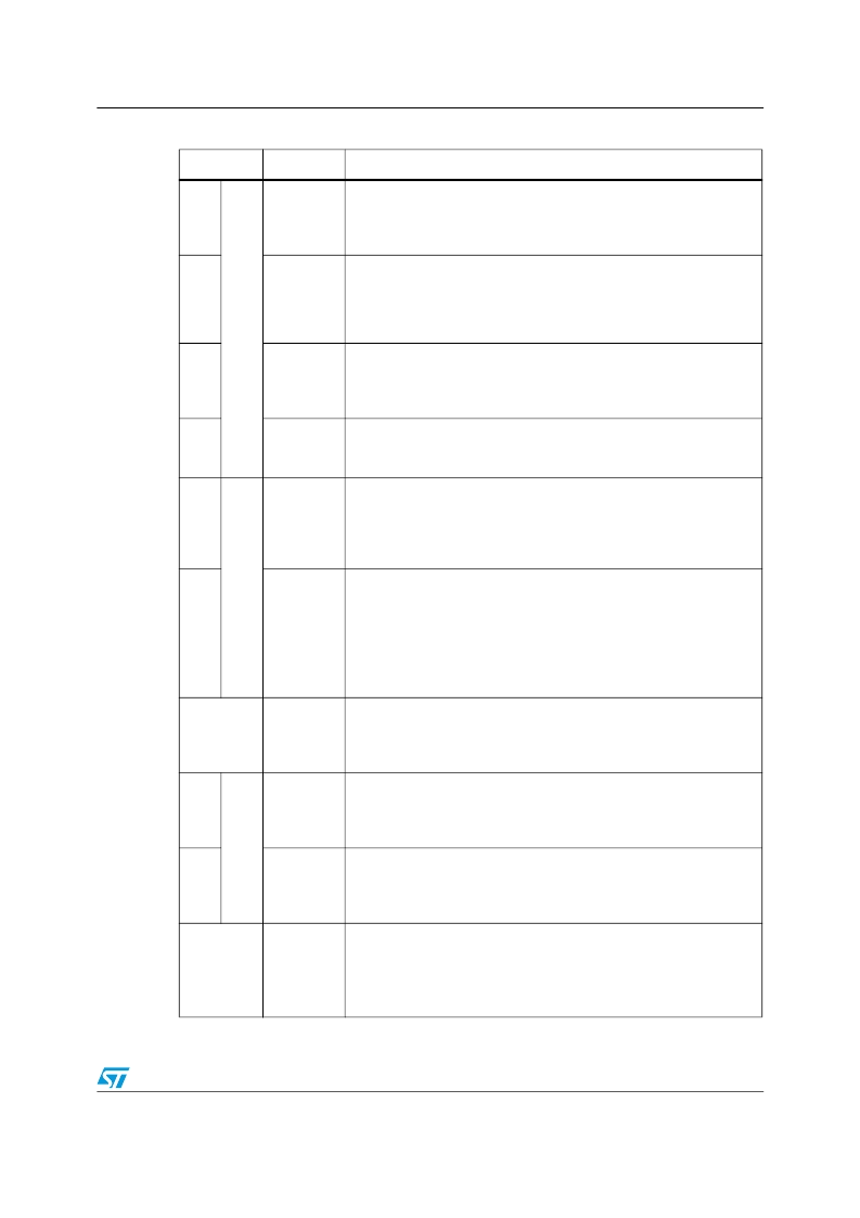
31
N
NB_VSEN
NB output voltage monitor.
It manages OVP and UVP protections and PWRGOOD. Connect to the
positive side of the NB load to perform remote sensing. See
Section 9
for proper layout of this connection.
32
NB_DROOP
A current proportional to the total current read by the NB section is
sourced through this pin according to the Current Reading Gain
(R
ISEN
). Short to NB_FB to implement Droop Function or connect to
SGND through a resistor and filter with 1nF capacitor to implement NB
LOAD Indicator. If not used, short to SGND.
33
NB_FB
NB error amplifier inverting input.
Connect with a resistor R
FB_NB
to NB_VSEN and with an R
F_NB
- C
F_NB
to NB_COMP. Offset current programmed by NB_OS is sunk through
this pin.
34
NB_COMP
Error amplifier output.
Connect with an R
F_NB
- C
F_NB
to NB_FB. The NB Section or the device
cannot be disabled by grounding this pin.
35,
36
S
VID0, VID1
Voltage IDentification Pins.
Internally pulled-low by 10
μ
A, they are used to program the output
voltage. VID1 is monitored on the EN pin rising-edge to define the
operative mode of the controller (SVI or PVI). When in SVI Mode, VID0
is ignored. See
Section 5
for details.
37
PWROK
System-wide Power Good Input (SVI Mode).
Internally pulled-low by 10
μ
A. When low, the device will decode the two
SVI bits (SVC, SVD) to determine the
Pre-PWROK Metal VID
(default
condition when pin is floating).
When high, the device will actively run the SVI protocol.
Pre-PWROK Metal VID
are latched after EN is asserted and re-used in
case of PWROK de-assertion. Latch is reset by VCC or EN cycle.
38
EN
VR Enable. Internally pulled-up to 3.3V by 10
μ
A.
Pull-low to disable the device. When set free, the device immediately
checks for the VID1 status to determine the SVI / PVI protocol to be
adopted and configures itself accordingly. See
Section 5
for details.
39
S
SVC / VID3
Voltage IDentification Pin - SVI Clock Pin.
Internally pulled-low by 10
μ
A, it is used to program the output voltage.
When in SVI-Mode, it is considered as Serial-VID-Data (Input / Open
Drain Output). See
Section 5
for details.
40
SVD / VID2
Voltage IDentification Pins - SVI Data Pin.
Internally pulled-low by 10
μ
A, it is used to program the output voltage.
When in SVI-Mode, it is considered as Serial-VID-Data (Input / Open
Drain Output). See
Section 5
for details.
41
PWRGOOD
VCORE and NB Power Good.
It is an open-drain output set free after SS as long as both the voltage
planes are within specifications. Pull-up to 3.3V (typ) or lower, if not
used it can be left floating.
When in PVI Mode, it monitors the CORE Section only.
Table 2.
Pin description (continued)
Pin#
Name
Function
相關PDF資料 |
PDF描述 |
|---|---|
| L6741 | High current MOSFET driver |
| L6741TR | High current MOSFET driver |
| L6743 | High current MOSFET driver |
| L6743Q | High current MOSFET driver |
| L6919E | 5 BIT PROGRAMMABLE DUAL-PHASE CONTROLLER WITH DYNAMIC VID MANAGEMENT |
相關代理商/技術參數(shù) |
參數(shù)描述 |
|---|---|
| L6741 | 功能描述:功率驅動器IC SnglPphase Dual MOSFET Driver RoHS:否 制造商:Micrel 產(chǎn)品:MOSFET Gate Drivers 類型:Low Cost High or Low Side MOSFET Driver 上升時間: 下降時間: 電源電壓-最大:30 V 電源電壓-最小:2.75 V 電源電流: 最大功率耗散: 最大工作溫度:+ 85 C 安裝風格:SMD/SMT 封裝 / 箱體:SOIC-8 封裝:Tube |
| L6741TR | 功能描述:功率驅動器IC SnglPphase Dual MOSFET Driver RoHS:否 制造商:Micrel 產(chǎn)品:MOSFET Gate Drivers 類型:Low Cost High or Low Side MOSFET Driver 上升時間: 下降時間: 電源電壓-最大:30 V 電源電壓-最小:2.75 V 電源電流: 最大功率耗散: 最大工作溫度:+ 85 C 安裝風格:SMD/SMT 封裝 / 箱體:SOIC-8 封裝:Tube |
| L6743 | 功能描述:功率驅動器IC SnglPphase Dual MOSFET Driver RoHS:否 制造商:Micrel 產(chǎn)品:MOSFET Gate Drivers 類型:Low Cost High or Low Side MOSFET Driver 上升時間: 下降時間: 電源電壓-最大:30 V 電源電壓-最小:2.75 V 電源電流: 最大功率耗散: 最大工作溫度:+ 85 C 安裝風格:SMD/SMT 封裝 / 箱體:SOIC-8 封裝:Tube |
| L6743_08 | 制造商:STMICROELECTRONICS 制造商全稱:STMicroelectronics 功能描述:High current MOSFET driver |
| L6743B | 功能描述:功率驅動器IC Hi-current MOSFET Driver RoHS:否 制造商:Micrel 產(chǎn)品:MOSFET Gate Drivers 類型:Low Cost High or Low Side MOSFET Driver 上升時間: 下降時間: 電源電壓-最大:30 V 電源電壓-最小:2.75 V 電源電流: 最大功率耗散: 最大工作溫度:+ 85 C 安裝風格:SMD/SMT 封裝 / 箱體:SOIC-8 封裝:Tube |
發(fā)布緊急采購,3分鐘左右您將得到回復。