- 您現(xiàn)在的位置:買賣IC網(wǎng) > PDF目錄384590 > LCZM (Linear Technology Corporation) 16-/14-/12-Bit VOUT DACs in 3mm 】 3mm DFN PDF資料下載
參數(shù)資料
| 型號: | LCZM |
| 廠商: | Linear Technology Corporation |
| 英文描述: | 16-/14-/12-Bit VOUT DACs in 3mm 】 3mm DFN |
| 中文描述: | 16/14/12 VOUT電源數(shù)模轉換器采用3mm DFN封裝】3毫米 |
| 文件頁數(shù): | 11/20頁 |
| 文件大小: | 317K |
| 代理商: | LCZM |
LTC2641/LTC2642
11
26412f
OPERATION
The digital-to-analog transfer function at the V
OUT
pin
is:
where k is the decimal equivalent of the binary DAC input
code, N is the resolution, and V
REF
is between 2.0V and
V
DD
(see Tables 1a, 1b and 1c).
The LTC2642 includes matched resistors that are tied to
an external amplifier to provide bipolar output swing (Fig-
ure 2). The bipolar transfer function at the RFB pin is:
V
k
N
2
V
OUT IDEAL
(
REF
)
=
(see Tables 2a, 2b and 2c).
V
V
k
N
OUT BIPOLAR IDEAL
_
REF
(
)
–
–
1
=
2
1
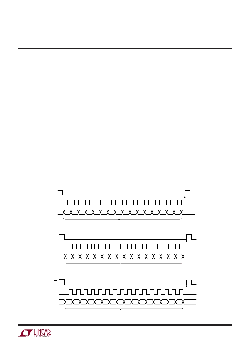
Serial Interface
The LTC2641/LTC2642 communicates via a standard
3-wire SPI/QSPI/MICROWIRE compatible interface. The
chip select input (
C
S) controls and frames the loading
of serial data from the data input (DIN). Following a
C
S
high-to-low transition, the data on DIN is loaded, MSB
first, into the shift register on each rising edge of the serial
clock input (SCLK). After 16 data bits have been loaded
into the serial input register, a low-to-high transition on
C
S
transfers the data to the 16-bit DAC latch, updating the DAC
output (see Figures 1a, 1b, 1c). While
C
S remains high,
the serial input shift register is disabled. If there are less
than 16 low-to-high transitions on SCLK while
C
S remains
low, the data will be corrupted, and must be reloaded.
Also, if there are more than 16 low-to-high transitions
on SCLK while
C
S remains low, only the last 16 data bits
loaded from DIN will be transferred to the DAC latch. For
the 14-bit DACs, (LTC2641-14/LTC2642-14), the MSB
remains in the same (left-justified) position in the input
16-bit data word. Therefore, two “don’t-care” bits must
be loaded after the LSB, to make up the required 16 data
bits (Figure 1b). Similarly, for the 12-bit family members
(LTC2641-12/LTC2642-12) four “don’t-care” bits must
follow the LSB (Figure 1c).
D15
MSB
1
CS
SCLK
DIN
2
3
4
5
6
7
8
9
10
11
12
13
14
15
16
D14
D13
D12
D11
D10
D9
D8
DATA (16 BITS)
D7
D6
D5
D4
D3
D2
D1
D0
LSB
DAC
UPDATED
26412 F01a
D13
MSB
1
CS
SCLK
DIN
2
3
4
5
6
7
8
9
10
11
12
13
14
15
16
D12
D11
D10
D9
D8
D7
D6
DATA (14 BITS + 2 DON’T-CARE BITS)
D5
D4
D3
D2
D1
D0
LSB
X
X
DAC
UPDATED
26412 F01b
MSB
1
CS
SCLK
DIN
2
3
4
5
6
7
8
9
10
11
12
13
14
15
16
D11
D10
D9
D8
D7
D6
DATA (12 BITS + 4 DON’T-CARE BITS)
Figure 1c. 12-Bit Timing Diagram (LTC2641-12/LTC2642-12)
D5
D4
D3
D2
D1
D0
LSB
X
X
X
X
DAC
UPDATED
26412 F01c
Figure 1b. 14-Bit Timing Diagram (LTC2641-14/LTC2642-14)
Figure 1a. 16-Bit Timing Diagram (LTC2641-16/LTC2642-16)
相關PDF資料 |
PDF描述 |
|---|---|
| LCZN | 16-/14-/12-Bit VOUT DACs in 3mm 】 3mm DFN |
| LCZP | 16-/14-/12-Bit VOUT DACs in 3mm 】 3mm DFN |
| LD1117-12-S08-B-R | 5.0 AMP POSITIVE VOLTAGE REGULATOR |
| LD1117-12-AA3-A-R | 5.0 AMP POSITIVE VOLTAGE REGULATOR |
| LD1117-12-AA3-B-R | 5.0 AMP POSITIVE VOLTAGE REGULATOR |
相關代理商/技術參數(shù) |
參數(shù)描述 |
|---|---|
| LCZN | 制造商:LINER 制造商全稱:Linear Technology 功能描述:16-/14-/12-Bit VOUT DACs in 3mm 】 3mm DFN |
| LCZP | 制造商:LINER 制造商全稱:Linear Technology 功能描述:16-/14-/12-Bit VOUT DACs in 3mm 】 3mm DFN |
| LD 1000 | 制造商:NOGA 功能描述:LEADER |
| LD 242-2/3 | 功能描述:紅外發(fā)射源 GaAs 950 nm MTL CAN HALF ANGLE +/-40DEG RoHS:否 制造商:Fairchild Semiconductor 波長:880 nm 射束角:+/- 25 輻射強度: 最大工作溫度:+ 100 C 最小工作溫度:- 40 C 封裝 / 箱體:Side Looker 封裝:Bulk |
| LD 260 | 功能描述:標準LED-通孔 Infrared 950nm HALF ANGLE +/-15DEG RoHS:否 制造商:Vishay Semiconductors 照明顏色:Red 光強度:0.7 mcd 波長/色溫:615 nm 顯示角:45 deg 透鏡顏色/類型:Clear, Non-Diffused 正向電流:70 mA 正向電壓:1.83 V to 3.03 V LED 大小:2 mm 系列: 封裝:Tube |
發(fā)布緊急采購,3分鐘左右您將得到回復。