- 您現(xiàn)在的位置:買賣IC網(wǎng) > PDF目錄362863 > M38C32M5AXXXFS (Mitsubishi Electric Corporation) SINGLE-CHIP 8-BIT CMOS MICROCOMPUTER PDF資料下載
參數(shù)資料
| 型號(hào): | M38C32M5AXXXFS |
| 廠商: | Mitsubishi Electric Corporation |
| 英文描述: | SINGLE-CHIP 8-BIT CMOS MICROCOMPUTER |
| 中文描述: | 單芯片8位CMOS微機(jī) |
| 文件頁數(shù): | 27/62頁 |
| 文件大小: | 881K |
| 代理商: | M38C32M5AXXXFS |
第1頁第2頁第3頁第4頁第5頁第6頁第7頁第8頁第9頁第10頁第11頁第12頁第13頁第14頁第15頁第16頁第17頁第18頁第19頁第20頁第21頁第22頁第23頁第24頁第25頁第26頁當(dāng)前第27頁第28頁第29頁第30頁第31頁第32頁第33頁第34頁第35頁第36頁第37頁第38頁第39頁第40頁第41頁第42頁第43頁第44頁第45頁第46頁第47頁第48頁第49頁第50頁第51頁第52頁第53頁第54頁第55頁第56頁第57頁第58頁第59頁第60頁第61頁第62頁
27
SINGLE-CHIP 8-BIT CMOS MICROCOMPUTER
MITSUBISHI MICROCOMPUTERS
38C3 Group
LCD DRIVE CONTROL CIRCUIT
The 38C3 group has the built-in Liquid Crystal Display (LCD) drive
control circuit consisting of the following.
LCD display RAM
Segment output enable register
LCD mode register
Selector
Timing controller
Common driver
Segment driver
Bias control circuit
A maximum of 32 segment output pins and 4 common output pins
can be used.
Up to 128 pixels can be controlled for a LCD display. When the LCD
enable bit is set to “1” after data is set in the LCD mode register, the
Fig. 27 Structure of LCD related registers
segment output enable register, and the LCD display RAM, the LCD
drive control circuit starts reading the display data automatically, per-
forms the bias control and the duty ratio control, and displays the
data on the LCD panel.
Table 7 Maximum number of display pixels at each duty ratio
Duty ratio
1
2
3
4
Maximum number of display pixels
32 dots
or 8 segment LCD 4 digits
64 dots
or 8 segment LCD 8 digits
96 dots
or 8 segment LCD 12 digits
128 dots
or 8 segment LCD 16 digits
Segment output enable bit 0
0 : I/O ports P2
0
–P2
3
1 : Segment output SEG
0
–SEG
3
Segment output enable bit 1
0 : I/O ports P2
4
–P2
7
1 : Segment output SEG
4
–SEG
7
Segment output enable bit 2
0 : I/O ports P0
0
–P0
3
1 : Segment output SEG
8
–SEG
11
Segment output enable bit 3
0 : I/O ports P0
4
–P0
7
1 : Segment output SEG
12
–SEG
15
Segment output enable bit 4
0 : I/O ports P1
0
–P1
3
1 : Segment output SEG
16
–SEG
19
Segment output enable bit 5
0 : I/O ports P1
4
–P1
7
1 : Segment output SEG
20
–SEG
23
Segment output enable bit 6
0 : Output ports P3
0
–P3
3
1 : Segment output SEG
24
–SEG
27
Segment output enable bit 7
0 : Output ports P3
4
–P3
7
1 : Segment output SEG
28
–SEG
31
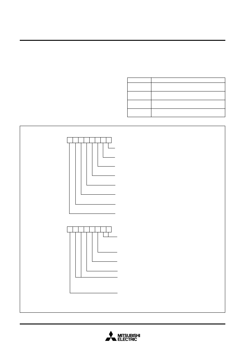
Segment output enable register
(SEG : address 0038
16
)
b7
b0
LCD mode register
(LM : address 0039
16
)
Duty ratio selection bits
0 0 : 1 (use COM
0
)
0 1 : 2 (use COM
0
,COM
1
)
1 0 : 3 (use COM
0
–COM
2
)
1 1 : 4 (use COM
0
–COM
3
)
Bias control bit
0 : 1/3 bias
1 : 1/2 bias
LCD enable bit
0 : LCD OFF
1 : LCD ON
Not used (returns “0” when read)
(Do not write “1” to this bit.)
LCD circuit divider division ratio selection bits
0 0 : Clock input
0 1 : 2 division of clock input
1 0 : 4 division of clock input
1 1 : 8 division of clock input
LCDCK count source selection bit
(Note)
0 : f(X
CIN
)/32
1 : f(X
IN
)/8192 (f(X
CIN
)/8192 in low-speed mode)
Note :
LCDCK is a clock for a LCD timing controller.
b7
b0
相關(guān)PDF資料 |
PDF描述 |
|---|---|
| M38C32M5MXXXFP | SINGLE-CHIP 8-BIT CMOS MICROCOMPUTER |
| M38C32M5MXXXFS | SINGLE-CHIP 8-BIT CMOS MICROCOMPUTER |
| M38C33M2AXXXFP | SINGLE-CHIP 8-BIT CMOS MICROCOMPUTER |
| M38C33M2AXXXFS | ECONOLINE: RSZ/P - 1kVDC |
| M38C33M2MXXXFP | SINGLE-CHIP 8-BIT CMOS MICROCOMPUTER |
相關(guān)代理商/技術(shù)參數(shù) |
參數(shù)描述 |
|---|---|
| M38C32M5M | 制造商:RENESAS 制造商全稱:Renesas Technology Corp 功能描述:SINGLE-CHIP 8-BIT CMOS MICROCOMPUTER |
| M38C32M5MXXXFP | 制造商:MITSUBISHI 制造商全稱:Mitsubishi Electric Semiconductor 功能描述:SINGLE-CHIP 8-BIT CMOS MICROCOMPUTER |
| M38C32M5MXXXFS | 制造商:MITSUBISHI 制造商全稱:Mitsubishi Electric Semiconductor 功能描述:SINGLE-CHIP 8-BIT CMOS MICROCOMPUTER |
| M38C32M6A | 制造商:RENESAS 制造商全稱:Renesas Technology Corp 功能描述:SINGLE-CHIP 8-BIT CMOS MICROCOMPUTER |
| M38C32M6AXXXFP | 制造商:MITSUBISHI 制造商全稱:Mitsubishi Electric Semiconductor 功能描述:SINGLE-CHIP 8-BIT CMOS MICROCOMPUTER |
發(fā)布緊急采購,3分鐘左右您將得到回復(fù)。