- 您現(xiàn)在的位置:買賣IC網(wǎng) > PDF目錄16675 > AD633-EVALZ (Analog Devices Inc)BOARD EVAL FOR AD633 PDF資料下載
參數(shù)資料
| 型號: | AD633-EVALZ |
| 廠商: | Analog Devices Inc |
| 文件頁數(shù): | 2/21頁 |
| 文件大小: | 0K |
| 描述: | BOARD EVAL FOR AD633 |
| 標準包裝: | 1 |
| 主要目的: | 模擬乘法器 |
| 嵌入式: | 否 |
| 已用 IC / 零件: | AD633 |
| 主要屬性: | 四象限乘法 |
| 已供物品: | 板 |

Data Sheet
AD633
Rev. J | Page 9 of 20
APPLICATIONS INFORMATION
The AD633 is well suited for such applications as modulation
and demodulation, automatic gain control, power measurement,
voltage-controlled amplifiers, and frequency doublers. These
applications show the pin connections for the AD633JN (8-lead
PDIP), which differs from the AD633JR (8-lead SOIC).
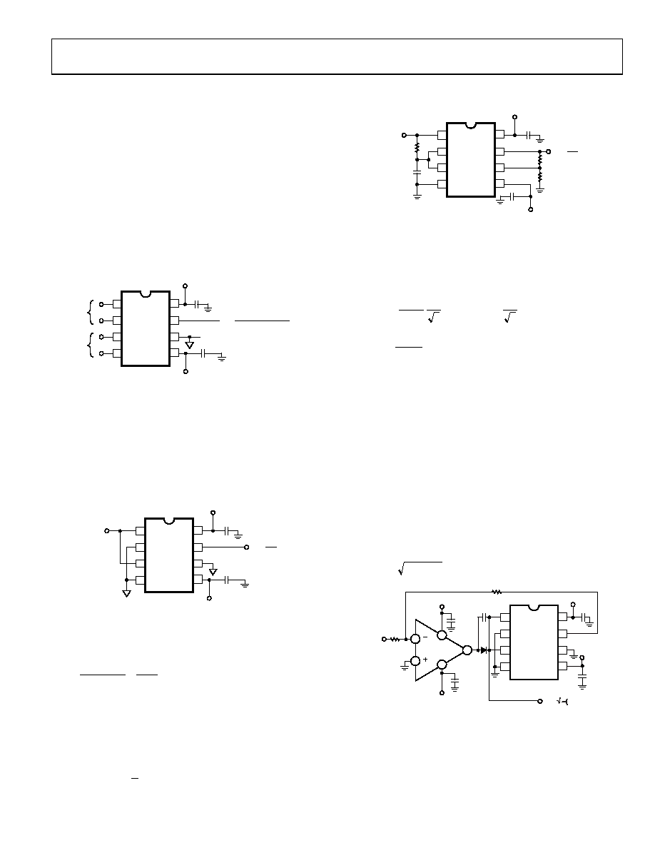
MULTIPLIER CONNECTIONS
Figure 12 shows the basic connections for multiplication. The X
and Y inputs normally have their negative nodes grounded, but
they are fully differential, and in many applications, the grounded
inputs may be reversed (to facilitate interfacing with signals of a
particular polarity while achieving some desired output polarity),
or both may be driven.
AD633JN
X1
1
X2
2
Y1
3
Y2
4
+VS 8
W 7
Z 6
–VS 5
X
INPUT
Y
INPUT
+
–
+
–
0.1F
+15V
–15V
OPTIONAL SUMMING
INPUT, Z
W =
+ Z
(X1 – X2)(Y1 – Y2)
10V
00
78
6-
0
1
Figure 12. Basic Multiplier Connections
SQUARING AND FREQUENCY DOUBLING
As is shown in Figure 13, squaring of an input signal, E, is
achieved simply by connecting the X and Y inputs in parallel to
produce an output of E2/10 V. The input can have either polarity,
but the output is positive. However, the output polarity can be
reversed by interchanging the X or Y inputs. The Z input can be
used to add a further signal to the output.
AD633JN
X1
1
E
X2
2
Y1
3
Y2
4
+VS 8
W 7
Z 6
–VS 5
0.1F
+15V
–15V
W =
E2
10V
007
86
-01
2
Figure 13. Connections for Squaring
When the input is a sine wave E sin ωt, this squarer behaves as a
frequency doubler, because
t
V
E
V
t
E
2
cos
1
20
10
sin
2
(2)
Equation 2 shows a dc term at the output that varies strongly
with the amplitude of the input, E. This can be avoided using
the connections shown in Figure 14, where an RC network is
used to generate two signals whose product has no dc term. It
uses the identity
θ
θ
2
sin
2
1
sin
cos
(3)
AD633JN
X1
1
X2
2
Y1
3
Y2
4
+VS 8
W 7
Z 6
–VS 5
0.1F
+15V
–15V
W =
E2
10V
00
78
6-
01
3
E
R
C
R2
3k
R1
1k
Figure 14. Bounceless Frequency Doubler
At ωo = 1/CR, the X input leads the input signal by 45° (and is
attenuated by √2), and the Y input lags the X input by 45° (and
is also attenuated by √2). Because the X and Y inputs are 90° out of
phase, the response of the circuit is (satisfying Equation 3)
45
sin
2
45
sin
2
10
1
0
t
E
t
E
V
W
t
V
E
0
2
sin
40
(4)
which has no dc component. Resistors R1 and R2 are included
to restore the output amplitude to 10 V for an input amplitude
of 10 V.
The amplitude of the output is only a weak function of frequency;
the output amplitude is 0.5% too low at ω = 0.9 ω0 and ω0 = 1.1 ω0.
GENERATING INVERSE FUNCTIONS
Inverse functions of multiplication, such as division and square
rooting, can be implemented by placing a multiplier in the feedback
loop of an op amp. Figure 15 shows how to implement square
rooting with the transfer function for the condition E < 0.
The 1N4148 diode is required to prevent latchup, which can
occur in such applications if the input were to change polarity,
even momentarily.
V
E
W
10
(5)
AD633JN
X1
1
X2
2
Y1
3
Y2
4
+VS 8
W 7
Z 6
–VS 5
0.1F
E < 0V
–15V
+15V
AD711
0.1F
10k
000
78
6-
01
4
0.1F
W = √ –(10V)E
0.01F
+15V
–15V
7
4
3
6
2
0.1F
1N4148
Figure 15. Connections for Square Rooting
相關(guān)PDF資料 |
PDF描述 |
|---|---|
| A8MMS-1018G | ADM10S/AE10G/ADM10S |
| M3DDA-1406R | IDC CABLE - MKR14A/MC14M/MKR14A |
| EEC10DREI-S93 | CONN EDGECARD 20POS .100 EYELET |
| EVAL-ADMP441Z-FLEX | EVAL BOARD FOR ADMP441 |
| SRR6038-330Y | INDUCTOR POWER 33UH 1.1A SMD |
相關(guān)代理商/技術(shù)參數(shù) |
參數(shù)描述 |
|---|---|
| MC74HC273AFG | 功能描述:觸發(fā)器 2-6V CMOS Octal D-Type RoHS:否 制造商:Texas Instruments 電路數(shù)量:2 邏輯系列:SN74 邏輯類型:D-Type Flip-Flop 極性:Inverting, Non-Inverting 輸入類型:CMOS 輸出類型: 傳播延遲時間:4.4 ns 高電平輸出電流:- 16 mA 低電平輸出電流:16 mA 電源電壓-最大:5.5 V 最大工作溫度:+ 85 C 安裝風(fēng)格:SMD/SMT 封裝 / 箱體:X2SON-8 封裝:Reel |
| MC74HC273AH | 制造商:Rochester Electronics LLC 功能描述:- Bulk |
| MC74HC273AN | 功能描述:觸發(fā)器 2-6V CMOS Octal RoHS:否 制造商:Texas Instruments 電路數(shù)量:2 邏輯系列:SN74 邏輯類型:D-Type Flip-Flop 極性:Inverting, Non-Inverting 輸入類型:CMOS 輸出類型: 傳播延遲時間:4.4 ns 高電平輸出電流:- 16 mA 低電平輸出電流:16 mA 電源電壓-最大:5.5 V 最大工作溫度:+ 85 C 安裝風(fēng)格:SMD/SMT 封裝 / 箱體:X2SON-8 封裝:Reel |
| MC74HC273AND | 制造商:Motorola Inc 功能描述: |
| MC74HC273ANG | 功能描述:觸發(fā)器 2-6V CMOS Octal D-Type RoHS:否 制造商:Texas Instruments 電路數(shù)量:2 邏輯系列:SN74 邏輯類型:D-Type Flip-Flop 極性:Inverting, Non-Inverting 輸入類型:CMOS 輸出類型: 傳播延遲時間:4.4 ns 高電平輸出電流:- 16 mA 低電平輸出電流:16 mA 電源電壓-最大:5.5 V 最大工作溫度:+ 85 C 安裝風(fēng)格:SMD/SMT 封裝 / 箱體:X2SON-8 封裝:Reel |
發(fā)布緊急采購,3分鐘左右您將得到回復(fù)。