- 您現(xiàn)在的位置:買賣IC網(wǎng) > PDF目錄382783 > μPD30700 (NEC Corp.) 64-Bit Microprocessor(64位RISC微處理器) PDF資料下載
參數(shù)資料
| 型號: | μPD30700 |
| 廠商: | NEC Corp. |
| 英文描述: | 64-Bit Microprocessor(64位RISC微處理器) |
| 中文描述: | 64位微處理器(64位的RISC微處理器) |
| 文件頁數(shù): | 14/36頁 |
| 文件大?。?/td> | 210K |
| 代理商: | ΜPD30700 |
第1頁第2頁第3頁第4頁第5頁第6頁第7頁第8頁第9頁第10頁第11頁第12頁第13頁當(dāng)前第14頁第15頁第16頁第17頁第18頁第19頁第20頁第21頁第22頁第23頁第24頁第25頁第26頁第27頁第28頁第29頁第30頁第31頁第32頁第33頁第34頁第35頁第36頁
μ
PD30500, 30500A, 30500B
14
Data Sheet U12031EJ4V0DS00
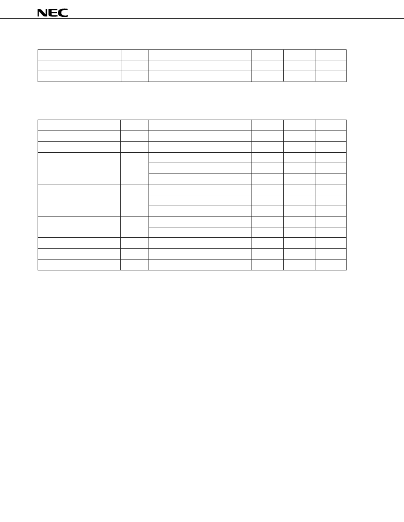
Capacitance
Parameter
Symbol
Condition
MIN.
MAX.
Unit
Input capacitance
C
In
5
pF
Output capacitance
C
out
7
pF
AC Characteristics (T
C
= 0 to +70
°
C (PGA Package), T
C
= 0 to +85
°
C (BGA Package), V
DD
= 3.3 V
±
5%)
Clock parameter
Parameter
Symbol
Condition
MIN.
MAX.
Unit
System clock high-level width
t
CH
3.0
ns
System clock low-level width
t
CL
3.0
ns
System clock frequency
Notes 1, 2
150 MHz
20
75
MHz
180 MHz
20
90
MHz
200 MHz
20
100
MHz
System clock cycle
t
CP
150 MHz
13.3
50
ns
180 MHz
11.1
50
ns
200 MHz
10
50
ns
System clock jitter
t
ji
System clock frequency > 66 MHz
±
125
ps
System clock frequency
≤
66 MHz
±
250
ps
System clock rise time
t
CR
2.0
ns
System clock fall time
t
CF
2.0
ns
Mode clock cycle
t
MOC
256
×
t
CP
ns
Notes 1.
The operation of the V
R
5000 is guaranteed only when the PLL is operating
2.
The operation is guaranteed if the internal operating frequency 100 MHz or higher.
相關(guān)PDF資料 |
PDF描述 |
|---|---|
| μPD30710 | 64-Bit Microprocessor(64位RISC微處理器) |
| μPD431000A-X | 1 M-Bit CMOS Static RAM(1M CMOS靜態(tài)RAM) |
| μPD431008 | 1M-Bit CMOS Fast Static RAM(1M位CMOS 快速靜態(tài)) |
| μPD431016 | 1M-Bit CMOS Fast Static RAM(1M位CMOS 快速靜態(tài)) |
| μPD434004 | 4M-Bit CMOS Fast Static RAM(4M位CMOS 快速靜態(tài)) |
相關(guān)代理商/技術(shù)參數(shù) |
參數(shù)描述 |
|---|---|
| PD308 | 制造商:NIEC 制造商全稱:Nihon Inter Electronics Corporation 功能描述:DIODE MODULE 30A/800V |
| PD30-CADG13 | 制造商:P-TEC 制造商全稱:P-tec Corporation 功能描述:Single Digit 7 Segment 4.0” LED Display |
| PD30-CADO12 | 制造商:P-TEC 制造商全稱:P-tec Corporation 功能描述:Single Digit 7 Segment 4.0” LED Display |
| PD30-CADR09 | 制造商:P-TEC 制造商全稱:P-tec Corporation 功能描述:Single Digit 7 Segment 4.0” LED Display |
| PD30-CADR21 | 制造商:P-TEC 制造商全稱:P-tec Corporation 功能描述:Single Digit 7 Segment 4.0” LED Display |
發(fā)布緊急采購,3分鐘左右您將得到回復(fù)。