- 您現(xiàn)在的位置:買賣IC網(wǎng) > PDF目錄382788 > μPD78070A (NEC Corp.) 8 Bit Single Chip Microcontrollers(8位單片微控制器) PDF資料下載
參數(shù)資料
| 型號: | μPD78070A |
| 廠商: | NEC Corp. |
| 英文描述: | 8 Bit Single Chip Microcontrollers(8位單片微控制器) |
| 中文描述: | 8位單片機(jī)微控制器(8位單片微控制器) |
| 文件頁數(shù): | 40/74頁 |
| 文件大小: | 481K |
| 代理商: | ΜPD78070A |
第1頁第2頁第3頁第4頁第5頁第6頁第7頁第8頁第9頁第10頁第11頁第12頁第13頁第14頁第15頁第16頁第17頁第18頁第19頁第20頁第21頁第22頁第23頁第24頁第25頁第26頁第27頁第28頁第29頁第30頁第31頁第32頁第33頁第34頁第35頁第36頁第37頁第38頁第39頁當(dāng)前第40頁第41頁第42頁第43頁第44頁第45頁第46頁第47頁第48頁第49頁第50頁第51頁第52頁第53頁第54頁第55頁第56頁第57頁第58頁第59頁第60頁第61頁第62頁第63頁第64頁第65頁第66頁第67頁第68頁第69頁第70頁第71頁第72頁第73頁第74頁
m
PD78070A
39
Resonator
Recommended
Parameter
Test Conditions
MIN.
TYP.
MAX.
Unit
Circuit
Ceramic
Oscillation frequency
V
DD
= Oscillation voltage
1.0
5.0
MHz
resonator
(f
X
)
Note1
range
Oscillation stabilization
After V
DD
came to MIN.
4
ms
time
Note2
of oscillation voltage range
Crystal
Oscillation frequency
1.0
5.0
MHz
resonator
(f
X
)
Note1
Oscillation stabilization
V
DD
= 4.5 to 5.5 V
10
ms
time
Note2
30
External clock
X1 input frequency
1.0
5.0
MHz
(f
X
)
Note1
X1 input high- and
85
500
ns
low-level widths (t
XH
, t
XL
)
Capacitance
(T
A
= 25 °C, V
DD
= V
SS
= 0 V)
Parameter
Test Conditions
MIN.
TYP.
MAX.
Unit
Input capacitance
C
IN
f = 1 MHz, Unmeasured pins returned to 0 V.
15
pF
Output capacitance
C
OUT
15
pF
I/O capacitance
C
IO
15
pF
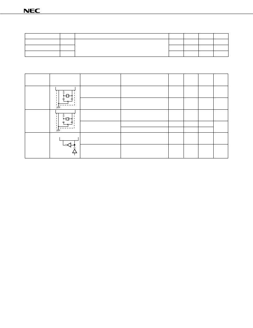
Main System Clock Oscillator Characteristics
(T
A
= –40 to +85 °C, V
DD
= 2.7 to 5.5 V)
Notes 1.
Only the oscillator characteristics are shown. For the instruction execution time, refer to
AC Characteristics
.
2.
Time required for oscillation to stabilize after a reset or the STOP mode has been released.
Cautions 1.
When using the oscillation circuit of the main system clock, wire the portion enclosed in dotted lines
in the figures as follows to avoid adverse influences on the wiring capacitance:
Keep the wiring length as short as possible.
Do not cross the wiring over other signal lines.
Do not route the wiring in the vicinity of lines through which a high fluctuating current flows.
Always keep the ground point of the capacitor of the oscillation circuit at the same potential as
V
SS
.
Do not connect the power source to a ground pattern through which a high current flows.
Do not extract signals from the oscillation circuit.
2.
When the main system clock is stopped and the device is operating on the subsystem clock, wait
until the oscillation stabilization time has been secured by the program before switching back to
the main system clock.
X2
X1
PD74HCU04
μ
IC
C1
X1
C2
R1
X2
IC
C1
X1
C2
R1
X2
相關(guān)PDF資料 |
PDF描述 |
|---|---|
| μPD78075B | 8 Bit Single Chip Microcontrollers |
| μPD78074B | 8 Bit Single Chip Microcontrollers(8位單片微控制器) |
| μPD78078Y | 8 Bit Single Chip Microcontrollers |
| μPD78076Y | 8 Bit Single Chip Microcontrollers(8位單片微控制器) |
| μPD78081(A) | 8 Bit Single Chip Microcontrollers(8位單片微控制器) |
相關(guān)代理商/技術(shù)參數(shù) |
參數(shù)描述 |
|---|---|
| PD7-80-70A | 制造商:MERRIMAC 制造商全稱:MERRIMAC 功能描述:0 , 75 ohm POWER DIVIDERS / COMBINERS |
| PD784054GCA2 | 制造商:NEC 制造商全稱:NEC 功能描述:16-BIT SINGLE-CHIP MICROCONTROLLER |
| PD784976A | 制造商:NEC 制造商全稱:NEC 功能描述:16-Bit Single-Chip Microcontroller |
| PD7869 | 制造商:未知廠家 制造商全稱:未知廠家 功能描述:Optoelectronic |
| PD78F0134 | 制造商:NEC 制造商全稱:NEC 功能描述:8-Bit Single-Chip Microcontrollers |
發(fā)布緊急采購,3分鐘左右您將得到回復(fù)。