- 您現(xiàn)在的位置:買賣IC網(wǎng) > PDF目錄368690 > 100311 (Fairchild Semiconductor Corporation) Low Skew 1:9 Differential Clock Driver PDF資料下載
參數(shù)資料
| 型號: | 100311 |
| 廠商: | Fairchild Semiconductor Corporation |
| 英文描述: | Low Skew 1:9 Differential Clock Driver |
| 中文描述: | 低偏移1:9差分時鐘驅(qū)動器 |
| 文件頁數(shù): | 3/6頁 |
| 文件大小: | 64K |
| 代理商: | 100311 |
3
www.fairchildsemi.com
1
Commercial Version
(Continued)
AC Electrical Characteristics
V
EE
=
4.2V to
5.7V, V
CC
=
V
CCA
=
GND
Note 4:
f
MAX
=
the highest frequency at which output V
OL
/V
OH
levels still meet V
IN
specifications. The F311 will function @ 1 GHz.
Note 5:
t
PS
describes opposite edge skews, i.e. the difference between the delay of a differential output signal pair
’
s LOW-to-HIGH and HIGH-to-LOW prop-
agation delays. With differential signal pairs, a LOW-to-HIGH or HIGH-to-LOW transition is defined as the transition of the true output or input pin.
Note 6:
t
OSLH
describes in-phase gate-to-gate differential propagation skews with all differential outputs going LOW-to-HIGH; t
OSHL
describes the same con-
ditions except with the outputs going HIGH-to-LOW.
Note 7:
t
OST
describes the maximum worst case difference in any of the t
PS
, t
OSLH
or t
OST
delay paths combined.
Note 8:
The skew specifications pertain to differential I/O paths.
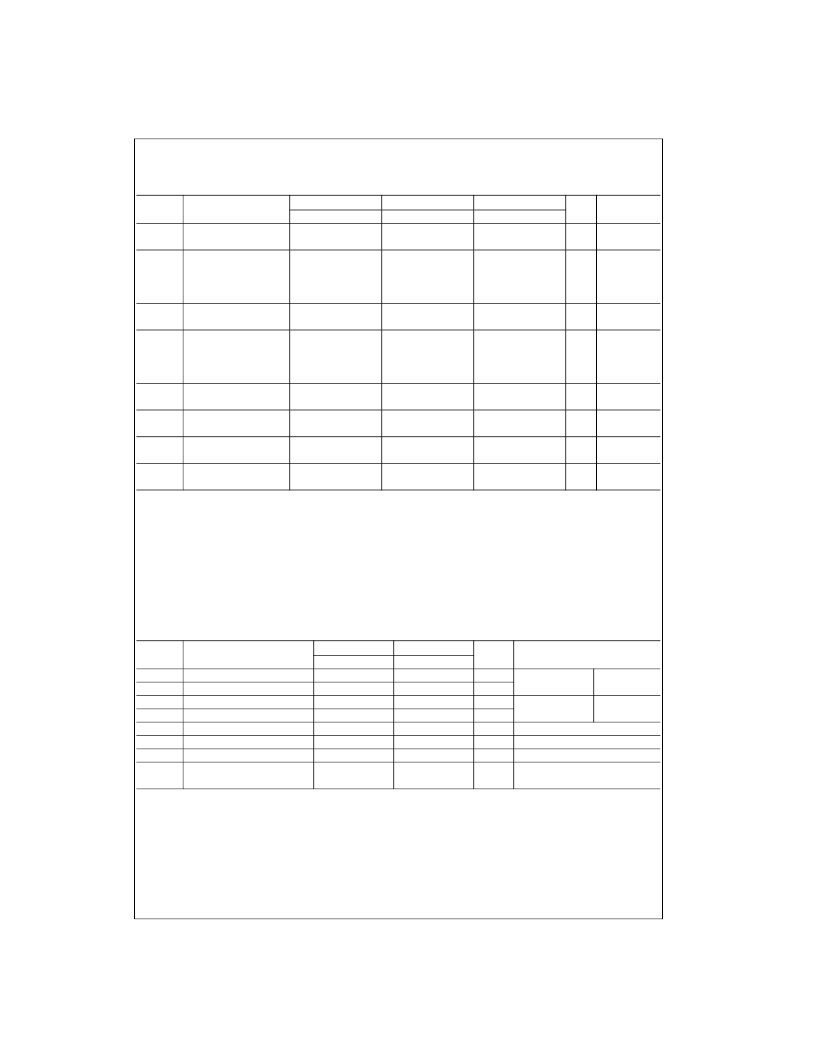
Industrial Version
DC Electrical Characteristics
(Note 9)
V
EE
=
4.2V to
5.7V, V
CC
=
V
CCA
=
GND, T
C
=
40
°
C to
+
85
°
C
Symbol
Parameter
T
C
=
0
°
C
Typ
T
C
=
+
25
°
C
Typ
T
C
=
+
85
°
C
Typ
Units
Conditions
Min
750
Max
Min
750
Max
Min
750
Max
f
MAX
Max Toggle Frequency
CLKIN to Q
n
Propagation Delay,
MHz
(Note 4)
t
PLH
t
PHL
CLKIN
n
to CLK
n
Differential
Single-Ended
0.75
0.65
0.84
0.90
0.95
1.05
0.75
0.67
0.86
0.93
0.95
1.17
0.84
0.74
0.93
1.06
1.04
1.24
ns
Figure 3
t
PLH
t
PHL
t
PS
t
OSLH
t
OSHL
t
OST
t
S
Propagation Delay
SEL to Output
LH
–
HL Skew
0.75
1.03
1.20
0.80
1.05
1.25
0.85
1.12
1.35
ns
Figure 2
10
30
10
30
10
30
ps
(Note 5)(Note 8)
Gate
–
Gate Skew LH
Gate
–
Gate Skew HL
Gate
–
Gate LH
–
HL Skew
20
20
30
50
50
60
20
20
30
50
50
60
20
20
30
50
50
60
(Note 6)(Note 8)
(Note 6)(Note 8)
(Note 7)(Note 8)
Setup Time
EN
n
to CLKIN
n
Hold Time
250
250
300
ps
t
H
0
0
0
ps
EN
n
to CLKIN
n
Release Time
EN
n
to CLKIN
n
Transition Time
20% to 80%, 80% to 20%
t
R
300
300
300
ps
t
TLH
t
THL
275
500
750
275
480
750
275
460
750
ps
Figure 4
Symbol
Parameter
T
C
=
40
°
C
Min
1085
1830
1095
T
C
=
0
°
C to
+
85
°
C
Min
1025
1830
1035
Units
Conditions
Max
870
1575
Max
870
1620
V
OH
V
OL
V
OHC
V
OLC
V
BB
V
DIFF
V
CM
V
IH
Output HIGH Voltage
Output LOW Voltage
Output HIGH Voltage
mV
mV
mV
V
IN
=
V
IH
(Max)
or V
IL
(Min)
V
IN
=
V
IH
or V
IL
(Min)
I
VBB
=
300
μ
A
Required for Full Output Swing
Loading with
50
to
2.0V
Loading with
50
to
2.0V
Output LOW Voltage
Output Reference Voltage
Input Voltage Differential
1565
1255
1610
1260
mV
mV
mV
1395
150
V
CC
2.0 V
CC
0.5 V
CC
2.0 V
CC
0.5
1170
870
1380
150
Common Mode Voltage
Input HIGH Voltage
V
1165
870
mV
Guaranteed HIGH Signal for
All Inputs
相關(guān)PDF資料 |
PDF描述 |
|---|---|
| 100311QC | Low Skew 1:9 Differential Clock Driver |
| 100311QI | Low Skew 1:9 Differential Clock Driver |
| 100313 | Low Power Quad Driver |
| 100313D | Low Power Quad Driver |
| 100313F | SLK 10-EX |
相關(guān)代理商/技術(shù)參數(shù) |
參數(shù)描述 |
|---|---|
| 100311_YAC3026T WAF | 制造商:Fairchild Semiconductor Corporation 功能描述: |
| 1003110000 | 制造商:Weidmuller 功能描述:CONN ENCLOSURE SIZE HQ |
| 100311020 | 制造商:ROSE+BOPLA (Pheonix Meanco) 功能描述:BRACKETS EXT 02 SERIES |
| 10031109-NFB28LF | 功能描述:板對板與夾層連接器 MF-730 RoHS:否 制造商:JAE Electronics 系列:WP3 產(chǎn)品類型:Receptacles 節(jié)距:0.4 mm 疊放高度:1 mm 安裝角: 位置/觸點數(shù)量:50 排數(shù):2 外殼材料:Plastic 觸點材料:Copper Alloy 觸點電鍍:Gold 電壓額定值:50 V 電流額定值:0.4 A |
| 1003119-1 | 制造商:OMNIMOUNT 功能描述:FEMALE ADAPTER |
發(fā)布緊急采購,3分鐘左右您將得到回復。