- 您現(xiàn)在的位置:買賣IC網(wǎng) > PDF目錄368770 > 1N5366BG (ON SEMICONDUCTOR) 5 Watt Surmetic TM 40 Zener Voltage Regulators PDF資料下載
參數(shù)資料
| 型號(hào): | 1N5366BG |
| 廠商: | ON SEMICONDUCTOR |
| 元件分類: | 參考電壓二極管 |
| 英文描述: | 5 Watt Surmetic TM 40 Zener Voltage Regulators |
| 中文描述: | 39 V, 5 W, SILICON, UNIDIRECTIONAL VOLTAGE REGULATOR DIODE |
| 封裝: | LEAD FREE, PLASTIC, CASE 017AA-01, 2 PIN |
| 文件頁數(shù): | 3/8頁 |
| 文件大小: | 88K |
| 代理商: | 1N5366BG |
1N5333B Series
http://onsemi.com
3
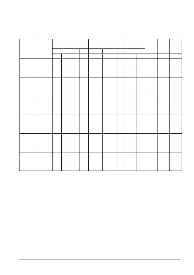
ELECTRICAL CHARACTERISTICS
(T
A
= 25
°
C unless otherwise noted, V
F
= 1.2 V Max @ I
F
= 1.0 A for all types)
Device
(Note 1)
Device
Marking
Zener Voltage
(Note 2)
Zener Impedance
(Note 2)
Leakage
Current
I
R
(Note 3)
V
Z
(Note 4)
I
ZM
(Note 5)
V
Z
(Volts)
@ I
ZT
Z
ZT
@ I
ZT
Z
ZK
@ I
ZK
I
ZK
I
R
@ V
R
Min
Nom
Max
mA
mA
A Max
Volts
A
Volts
mA
1N5333B, G
1N5334B, G
1N5335B, G
1N5336B, G
1N5337B, G
1N5333B
1N5334B
1N5335B
1N5336B
1N5337B
3.14
3.42
3.71
4.09
4.47
3.3
3.6
3.9
4.3
4.7
3.47
3.78
4.10
4.52
4.94
380
350
320
290
260
3
400
500
500
500
450
1
1
1
1
1
300
150
50
10
5
1
1
1
1
1
20
18.7
17.6
16.4
15.3
0.85
0.8
0.54
0.49
0.44
1440
1320
1220
1100
1010
2.5
2
2
2
1N5338B, G
1N5339B, G
1N5340B, G
1N5341B, G
1N5342B, G
1N5338B
1N5339B
1N5340B
1N5341B
1N5342B
4.85
5.32
5.70
5.89
6.46
5.1
5.6
6.0
6.2
6.8
5.36
5.88
6.30
6.51
7.14
240
220
200
200
175
1.5
1
1
1
1
400
400
300
200
200
1
1
1
1
1
1
1
1
1
1
2
3
3
14.4
13.4
12.7
12.4
11.5
0.39
0.25
0.19
0.1
0.15
930
865
790
765
700
10
5.2
1N5343B, G
1N5344B, G
1N5345B, G
1N5346B, G
1N5347B, G
1N5343B
1N5344B
1N5345B
1N5346B
1N5347B
7.13
7.79
8.27
8.65
9.50
7.5
8.2
8.7
9.1
10
7.88
8.61
9.14
9.56
10.5
175
150
150
150
125
1.5
1.5
2
2
2
200
200
200
150
125
1
1
1
1
1
10
10
10
7.5
5
5.7
6.2
6.6
6.9
7.6
10.7
10
9.5
9.2
8.6
0.15
0.2
0.2
0.22
0.22
630
580
545
520
475
1N5348B, G
1N5349B, G
1N5350B, G
1N5351B, G
1N5352B, G
1N5348B
1N5349B
1N5350B
1N5351B
1N5352B
10.45
11.4
12.35
13.3
14.25
11
12
13
14
15
11.55
12.6
13.65
14.7
15.75
125
100
100
100
75
2.5
2.5
2.5
2.5
2.5
125
125
100
75
75
1
1
1
1
1
5
2
1
1
1
8.4
9.1
9.9
10.6
11.5
8.0
7.5
7.0
6.7
6.3
0.25
0.25
0.25
0.25
0.25
430
395
365
340
315
1N5353B, G
1N5354B, G
1N5355B, G
1N5356B, G
1N5357B, G
1N5353B
1N5354B
1N5355B
1N5356B
1N5357B
15.2
16.15
17.1
18.05
19
16
17
18
19
20
16.8
17.85
18.9
19.95
21
75
70
65
65
65
2.5
2.5
2.5
3
3
75
75
75
75
75
1
1
1
1
1
1
12.2
12.9
13.7
14.4
15.2
6.0
5.8
5.5
5.3
5.1
0.3
0.35
0.4
0.4
0.4
295
280
264
250
237
0.5
0.5
0.5
0.5
1N5358B, G
1N5359B, G
1N5360B, G
1N5361B, G
1N5362B, G
1N5358B
1N5359B
1N5360B
1N5361B
1N5362B
20.9
22.8
23.75
25.65
26.6
22
24
25
27
28
23.1
25.2
26.25
28.35
29.4
50
50
50
50
50
3.5
3.5
4
5
6
75
100
110
120
130
1
1
1
1
1
0.5
0.5
0.5
0.5
0.5
16.7
18.2
19
20.6
21.2
4.7
4.4
4.3
4.1
3.9
0.45
0.55
0.55
0.6
0.6
216
198
190
176
170
Devices listed in
bold, italic
are ON Semiconductor
Preferred
devices.
Preferred
devices are recommended choices for future use and best overall value.
1.
TOLERANCE AND TYPE NUMBER DESIGNATION
The JEDEC type numbers shown indicate a tolerance of
±
5%.
2.
ZENER VOLTAGE (V
) and IMPEDANCE (I
and I
)
Test conditions for zener voltage and impedance are as follows: I
Z
is applied 40
±
10 ms prior to reading. Mounting contacts are located 3/8
″
to 1/2
″
from the inside edge of mounting clips to the body of the diode (T
A
= 25
°
C +8
°
C, 2
°
C).
3.
SURGE CURRENT (I
R
)
Surge current is specified as the maximum allowable peak, nonrecurrent squarewave current with a pulse width, PW, of 8.3 ms. The data
given in Figure 5 may be used to find the maximum surge current for a square wave of any pulse width between 1 ms and 1000 ms by plotting
the applicable points on logarithmic paper. Examples of this, using the 3.3 V and 200 V zener are shown in Figure 6. Mounting contact located
as specified in Note 2 (T
A
= 25
°
C +8
°
C, 2
°
C).
4.
VOLTAGE REGULATION ( V
Z
)
The conditions for voltage regulation are as follows: V
Z
measurements are made at 10% and then at 50% of the I
Z
max value listed in the
electrical characteristics table. The test current time duration for each V
Z
measurement is 40
±
10 ms. Mounting contact located as specified
in Note 2 (T
A
= 25
°
C +8
°
C, 2
°
C).
5.
MAXIMUM REGULATOR CURRENT (I
ZM
)
The maximum current shown is based on the maximum voltage of a 5% type unit, therefore, it applies only to the Bsuffix device. The actual
I
ZM
for any device may not exceed the value of 5 watts divided by the actual V
Z
of the device. T
L
= 75
°
C at 3/8
″
maximum from the device
body.
The “G’’ suffix indicates PbFree package available.
相關(guān)PDF資料 |
PDF描述 |
|---|---|
| 1N5366BRLG | 5 Watt Surmetic TM 40 Zener Voltage Regulators |
| 1N5367BG | 5 Watt Surmetic TM 40 Zener Voltage Regulators |
| 1N5355BRL | 5 Watt Surmetic 40 Zener Voltage Refulators |
| 1N5355BTA | 5 Watt Surmetic 40 Zener Voltage Refulators |
| 1N5355 | surface mount silicon Zener diodes |
相關(guān)代理商/技術(shù)參數(shù) |
參數(shù)描述 |
|---|---|
| 1N5366BRL | 功能描述:穩(wěn)壓二極管 39V 5W RoHS:否 制造商:Vishay Semiconductors 齊納電壓:12 V 電壓容差:5 % 電壓溫度系數(shù):0.075 % / K 齊納電流: 功率耗散:3 W 最大反向漏泄電流:3 uA 最大齊納阻抗:7 Ohms 最大工作溫度:+ 150 C 安裝風(fēng)格:SMD/SMT 封裝 / 箱體:DO-214AC 封裝:Reel |
| 1N5366BRLG | 功能描述:穩(wěn)壓二極管 39V 5W RoHS:否 制造商:Vishay Semiconductors 齊納電壓:12 V 電壓容差:5 % 電壓溫度系數(shù):0.075 % / K 齊納電流: 功率耗散:3 W 最大反向漏泄電流:3 uA 最大齊納阻抗:7 Ohms 最大工作溫度:+ 150 C 安裝風(fēng)格:SMD/SMT 封裝 / 箱體:DO-214AC 封裝:Reel |
| 1N5366B-T | 功能描述:穩(wěn)壓二極管 5.0W 39V RoHS:否 制造商:Vishay Semiconductors 齊納電壓:12 V 電壓容差:5 % 電壓溫度系數(shù):0.075 % / K 齊納電流: 功率耗散:3 W 最大反向漏泄電流:3 uA 最大齊納阻抗:7 Ohms 最大工作溫度:+ 150 C 安裝風(fēng)格:SMD/SMT 封裝 / 箱體:DO-214AC 封裝:Reel |
| 1N5366B-TP | 功能描述:穩(wěn)壓二極管 5.0W 39V RoHS:否 制造商:Vishay Semiconductors 齊納電壓:12 V 電壓容差:5 % 電壓溫度系數(shù):0.075 % / K 齊納電流: 功率耗散:3 W 最大反向漏泄電流:3 uA 最大齊納阻抗:7 Ohms 最大工作溫度:+ 150 C 安裝風(fēng)格:SMD/SMT 封裝 / 箱體:DO-214AC 封裝:Reel |
| 1N5366C/TR12 | 制造商:Microsemi Corporation 功能描述:5.0W, VZ = 39V, ? 2% - Tape and Reel 制造商:Microsemi Corporation 功能描述:DIODE ZENER 5.0W 39V 2% T-18 |
發(fā)布緊急采購,3分鐘左右您將得到回復(fù)。