- 您現(xiàn)在的位置:買(mǎi)賣(mài)IC網(wǎng) > PDF目錄351971 > 24C040-EST (Microchip Technology Inc.) 4K SPI ⑩ Bus Serial EEPROM PDF資料下載
參數(shù)資料
| 型號(hào): | 24C040-EST |
| 廠(chǎng)商: | Microchip Technology Inc. |
| 英文描述: | 4K SPI ⑩ Bus Serial EEPROM |
| 中文描述: | ⑩4K的的SPI總線(xiàn)串行EEPROM |
| 文件頁(yè)數(shù): | 5/12頁(yè) |
| 文件大小: | 240K |
| 代理商: | 24C040-EST |
25AA040/25LC040/25C040
DS21204A-page 2
Preliminary
1997 Microchip Technology Inc.
1.0
ELECTRICAL
CHARACTERISTICS
1.1
Maximum Ratings*
Vcc ...................................................................................7.0V
All inputs and outputs w.r.t. Vss.................. -0.6V to Vcc+1.0V
Storage temperature ....................................... -65C to 150C
Ambient temperature under bias..................... -65C to 125C
Soldering temperature of leads (10 seconds) ............. +300C
ESD protection on all pins................................................. 4kV
*Notice: Stresses above those listed under ‘Maximum ratings’ may
cause permanent damage to the device. This is a stress rating only and
functional operation of the device at those or any other conditions
above those indicated in the operational listings of this specication is
not implied. Exposure to maximum rating conditions for an extended
period of time may affect device reliability
TABLE 1-1:
PIN FUNCTION TABLE
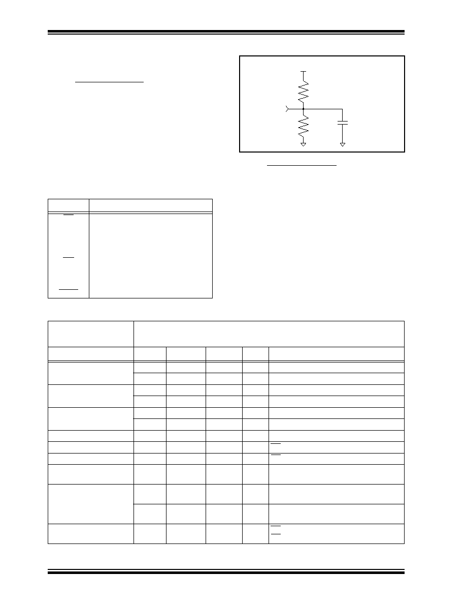
FIGURE 1-1:
AC TEST CIRCUIT
1.2
AC Test Conditions
Name
Function
CS
Chip Select Input
SO
Serial Data Output
SI
Serial Data Input
SCK
Serial Clock Input
WP
Write Protect Pin
VSS
Ground
VCC
Supply Voltage
HOLD
Hold Input
AC Waveform:
VLO = 0.2V
VHI = VCC - 0.2V
VHI = 4.0V
Timing Measurement Reference Level
Input
0.5 VCC
Output
0.5 VCC
Note 1: For VCC
≤ 4.0V
2: For VCC > 4.0V
VCC
SO
100 pF
1.8 K
2.25 K
TABLE 1-2:
DC CHARACTERISTICS
All parameters apply over the
specied operating ranges
unless otherwise noted.
Commercial (C): TAMB = 0
°C to +70°C
VCC = 1.8V to 5.5V
Industrial (I):
TAMB = -40
°C to +85°C
VCC = 1.8V to 5.5V
Automotive (E):
TAMB = -40
°C to +125°C
VCC = 4.5V to 5.5V (25C040 only)
Parameter
Symbol
Min
Max
Units
Test Conditions
High level input voltage
VIH1
2.0
VCC+1
V
VCC
≥ 2.7V (Note)
VIH2
0.7 VCC
VCC+1
V
VCC< 2.7V (Note)
Low level input voltage
VIL1
-0.3
0.8
V
VCC
≥ 2.7V (Note)
VIL2
-0.3
0.3 VCC
V
VCC < 2.7V (Note)
Low level output voltage
VOL
—
0.4
V
IOL = 2.1 mA
VOL
—
0.2
V
IOL = 1.0 mA, VCC < 2.5V
High level output voltage
VOH
VCC -0.5
—
V
IOH =-400
A
Input leakage current
ILI
-10
10
A
CS = VCC, VIN = VSS TO VCC
Output leakage current
ILO
-10
10
A
CS = VCC, VOUT = VSS TO VCC
Internal Capacitance
(all inputs and outputs)
CINT
—
7
pF
TAMB = 25C, CLK = 1.0 MHz,
VCC = 5.0V (Note)
Operating Current
ICC Read
—
1
500
mA
A
VCC = 5.5V; FCLK=3.0 MHz; SO = Open
VCC = 2.5V; FCLK=2.0 MHz; SO = Open
ICC Write
—
5
3
mA
VCC= 5.5V
VCC = 2.5V
Standby Current
ICCS
—
5
2
A
CS = Vcc = 5.5V, Inputs tied to VCC or VSS
CS = Vcc = 2.5V, Inputs tied to VCC or VSS
Note: This parameter is periodically sampled and not 100% tested.
相關(guān)PDF資料 |
PDF描述 |
|---|---|
| 24C04A-SN | 1K/2K/4K 5.0V I 2 C O Serial EEPROMs |
| 24LC160-P | 8K/16K 2.5V SPI O Bus Serial EEPROM |
| 24LC16B-IP | 16K 2.5V I 2 C O Serial EEPROM |
| 24LC16B-ISL | 16K 2.5V I 2 C O Serial EEPROM |
| 24LC16B-ISN | 16K 2.5V I 2 C O Serial EEPROM |
相關(guān)代理商/技術(shù)參數(shù) |
參數(shù)描述 |
|---|---|
| 24C040-IP | 制造商:MICROCHIP 制造商全稱(chēng):Microchip Technology 功能描述:4K SPI ⑩ Bus Serial EEPROM |
| 24C040-ISN | 制造商:MICROCHIP 制造商全稱(chēng):Microchip Technology 功能描述:4K SPI ⑩ Bus Serial EEPROM |
| 24C040-IST | 制造商:MICROCHIP 制造商全稱(chēng):Microchip Technology 功能描述:4K SPI ⑩ Bus Serial EEPROM |
| 24C040-P | 制造商:MICROCHIP 制造商全稱(chēng):Microchip Technology 功能描述:4K SPI ⑩ Bus Serial EEPROM |
| 24C040-SN | 制造商:MICROCHIP 制造商全稱(chēng):Microchip Technology 功能描述:4K SPI ⑩ Bus Serial EEPROM |
發(fā)布緊急采購(gòu),3分鐘左右您將得到回復(fù)。