- 您現(xiàn)在的位置:買賣IC網(wǎng) > PDF目錄368881 > 24LC024TIST I2C Serial EEPROM PDF資料下載
參數(shù)資料
| 型號: | 24LC024TIST |
| 英文描述: | I2C Serial EEPROM |
| 中文描述: | I2C串行EEPROM的 |
| 文件頁數(shù): | 7/12頁 |
| 文件大小: | 182K |
| 代理商: | 24LC024TIST |
24LC024/24LC025
1999 Microchip Technology Inc.
DS21210D-page 7
6.0
WRITE OPERATIONS
6.1
Byte Write
Following the start signal from the master, the device
code(4 bits), the chip select bits (3 bits), and the R/W
bit which is a logic low is placed onto the bus by the
master transmitter. The device will acknowledge this
control byte during the ninth clock pulse. The next byte
transmitted by the master is the word address and will
be written into the address pointer of the 24LC024/
24LC025. After receiving another acknowledge signal
from the 24LC024/24LC025 the master device will
transmit the data word to be written into the addressed
memory location. The 24LC024/24LC025 acknowl-
edges again and the master generates a stop condi-
tion. This initiates the internal write cycle, and during
this time the 24LC024/24LC025 will not generate
acknowledge signals (Figure 6-1). If an attempt is
made to write to the protected portion of the array when
the hardware write protection (24LC024 only) has been
enabled, the device will acknowledge the command but
no data will be written. The write cycle time must be
observed even if the write protection is enabled.
6.2
Page Write
The write control byte, word address and the first data
byte are transmitted to the 24LC024/24LC025 in the
same way as in a byte write. But instead of generating a
stop condition, the master transmits up to 15 additional
data bytes to the 24LC024/24LC025 which are tempo-
rarily stored in the on-chip page buffer and will be writ-
ten into the memory after the master has transmitted a
stop condition. After the receipt of each word, the four
lower order address pointer bits are internally incre-
mented by one. The higher order four bits of the word
address remains constant. If the master should transmit
more than 16 bytes prior to generating the stop condi-
tion, the address counter will roll over and the previously
received data will be overwritten. As with the byte write
operation, once the stop condition is received an inter-
nal write cycle will begin (Figure 6-2). If an attempt is
made to write to the protected portion of the array when
the hardware write protection has been enabled, the
device will acknowledge the command but no data will
be written. The write cycle time must be observed even
if the write protection is enabled.
6.3
WRITE PROTECTION
The WP pin (available on 24LC024 only) must be tied
to V
CC
or V
SS
. If tied to V
CC
, the entire array will be
write protected. If the WP pin is tied to V
SS
, then write
operations to all address locations are allowed.
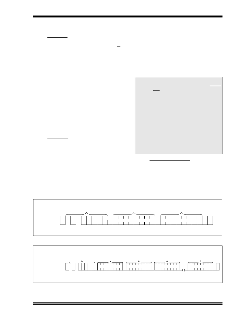
FIGURE 6-1:
BYTE WRITE
FIGURE 6-2:
PAGE WRITE
S
T
A
R
T
Note:
Page write operations are limited to writing
bytes within a single physical page, regard-
less of the number of bytes actually being
written. Physical page boundaries start at
addresses that are integer multiples of the
page buffer size (or ‘page size’) and end at
addresses that are integer multiples of
[page size - 1]. If a page write command
attempts to write across a physical page
boundary, the result is that the data wraps
around to the beginning of the current page
(overwriting data previously stored there),
instead of being written to the next page as
might be expected. It is therefore neces-
sary for the application software to prevent
page write operations that would attempt to
cross a page boundary.
S
P
BUS ACTIVITY
MASTER
SDA LINE
BUS ACTIVITY
S
T
A
R
T
S
T
O
P
CONTROL
BYTE
WORD
ADDRESS
DATA
A
C
K
A
C
K
A
C
K
S
P
BUS ACTIVITY
MASTER
SDA LINE
BUS ACTIVITY
CONTROL
BYTE
WORD
ADDRESS (n)
DATA n
DATA n + 15
S
T
O
P
A
C
K
A
C
K
A
C
K
A
C
K
A
C
K
DATA n +1
This Material Copyrighted by Its Respective Manufacturer
相關PDF資料 |
PDF描述 |
|---|---|
| 24LC024TSN | I2C Serial EEPROM |
| 24LC024TST | DS3/E3 Multiplexer Reference Design |
| 24LC025IP | I2C Serial EEPROM |
| 24LC025ISN | Ultraframer DS3/E3/DS2/E2/DS1/E1/DS0 |
| 24LC025IST | Ultraframer DS3/E3/DS2/E2/DS1/E1/DS0 |
相關代理商/技術參數(shù) |
參數(shù)描述 |
|---|---|
| 24LC024TSN | 制造商:未知廠家 制造商全稱:未知廠家 功能描述:I2C Serial EEPROM |
| 24LC024TST | 制造商:未知廠家 制造商全稱:未知廠家 功能描述:I2C Serial EEPROM |
| 24LC025 | 制造商:MICROCHIP 制造商全稱:Microchip Technology 功能描述:2K I2C? Serial EEPROM |
| 24LC025/P | 功能描述:電可擦除可編程只讀存儲器 256x8 RoHS:否 制造商:Atmel 存儲容量:2 Kbit 組織:256 B x 8 數(shù)據(jù)保留:100 yr 最大時鐘頻率:1000 KHz 最大工作電流:6 uA 工作電源電壓:1.7 V to 5.5 V 最大工作溫度:+ 85 C 安裝風格:SMD/SMT 封裝 / 箱體:SOIC-8 |
| 24LC025/SN | 功能描述:電可擦除可編程只讀存儲器 256x8 RoHS:否 制造商:Atmel 存儲容量:2 Kbit 組織:256 B x 8 數(shù)據(jù)保留:100 yr 最大時鐘頻率:1000 KHz 最大工作電流:6 uA 工作電源電壓:1.7 V to 5.5 V 最大工作溫度:+ 85 C 安裝風格:SMD/SMT 封裝 / 箱體:SOIC-8 |
發(fā)布緊急采購,3分鐘左右您將得到回復。