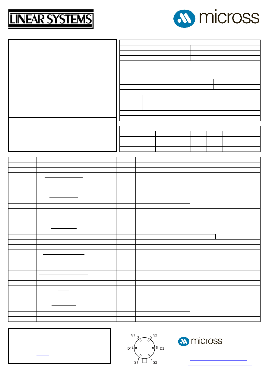
- 您現(xiàn)在的位置:買賣IC網(wǎng) > PDF目錄33242 > 2N3956-TO-78 (MICROSS COMPONENTS) 2 CHANNEL, N-CHANNEL, Si, SMALL SIGNAL, JFET, TO-78 PDF資料下載
參數(shù)資料
| 型號(hào): | 2N3956-TO-78 |
| 廠商: | MICROSS COMPONENTS |
| 元件分類: | 小信號(hào)晶體管 |
| 英文描述: | 2 CHANNEL, N-CHANNEL, Si, SMALL SIGNAL, JFET, TO-78 |
| 封裝: | HERMETIC SEALED, TO-78, 6 PIN |
| 文件頁(yè)數(shù): | 1/1頁(yè) |
| 文件大小: | 290K |
| 代理商: | 2N3956-TO-78 |

Information furnished by Linear Integrated Systems and Micross Components is believed to be accurate and reliable. However, no responsibility is assumed for its use; nor for any infringement of patents or
other rights of third parties which may result from its use. No license is granted by implication or otherwise under any patent or patent rights of Linear Integrated Systems.
FEATURES
LOWDRIFT
|VGS1‐2/T|=5V/°Cmax.
LOWLEAKAGE
IG=20pATYP.
LOWNOISE
en=10nV/√HzTYP.
ABSOLUTEMAXIMUMRATINGS
@25°C(unlessotherwisenoted)
MaximumTemperatures
StorageTemperature‐65°Cto+200°C
OperatingJunctionTemperature
+150°C
MaximumVoltageandCurrentforEachTransistor–Note1
‐VGSS
GateVoltagetoDrainorSource
60V
‐VDSO
DraintoSourceVoltage
60V
‐IG(f)
GateForwardCurrent
50mA
MaximumPowerDissipation
DeviceDissipation@FreeAir–Total400mW@25°C
MATCHINGCHARACTERISTICS@25°CUNLESSOTHERWISENOTED
SYMBOL
CHARACTERISTICS
VALUE
UNITS
CONDITIONS
|VGS1‐2/T|max.
DRIFTVS.
TEMPERATURE
50
V/°C
VDG=20V,ID=200A
TA=‐55°Cto+125°C
|VGS1‐2|max.
OFFSETVOLTAGE
15
mV
VDG=20V,ID=200A
ELECTRICALCHARACTERISTICS@25°C(unlessotherwisenoted)
SYMBOL
CHARACTERISTICS
MIN.
TYP.
MAX.
UNITS
CONDITIONS
BVGSS
BreakdownVoltage
60
‐‐
V
VDS=0ID=1A
BVGGO
YfSS
VDG=20VVGS=0Vf=1kHz
YfS
IDSS
VGS(off)orVp
GATEVOLTAGE
Pinchoffvoltage
1
2
4.5
V
VDS=20VID=1nA
VGS(on)
OperatingRange
0.5
‐‐
4
V
VDS=20VID=200A
‐IG
GATECURRENT
Operating
‐‐
20
50
pA
VDG=20VID=200A
‐IG
HighTemperature
‐‐
50
nA
TA=+125°C
‐IG
ReducedVDG
‐‐
5
‐‐
pA
VDG=10VID=200A
‐IGSS
AtFullConduction
‐‐
100
pA
VDG=20VVDS=0
YOSS
OUTPUTCONDUCTANCE
FullConduction
‐‐
‐‐
5
mho
VDG=20VVGS=0V
YOS
Operating
‐‐
0.1
1
mho
VDG=20VID=200A
|YOS1‐2|
Differential
‐‐
0.01
0.1
mho
CMR
COMMONMODEREJECTION
‐20log|VGS1‐2/VDS|
‐‐
100
‐‐
dB
VDS=10to20VID=200A
CMR‐20log|VGS1‐2/VDS|
‐‐
75
‐‐
dBVDS=5to10VID=200A
NF
NOISE
Figure
‐‐
‐‐
0.5
dB
VDS=20VVGS=0VRG=10MΩ
f=100HzNBW=6Hz
en
Voltage
‐‐
15
nV/√Hz
VDS=20VID=200Af=10HzNBW=1Hz
CISS
CAPACITANCE
Input
‐‐
‐‐
6
pF
VDS=20VVGS=0Vf=1MHz
CRSS
ReverseTransfer
‐‐
2
pF
CDD
Drain‐to‐Drain
‐‐
0.1
‐‐
pF
VDG=20VID=200A
The 2N3956 is a Low Noise, Low Drift, Monolithic Dual N-Channel JFET
2N3956
MONOLITHIC DUAL
N-CHANNEL JFET
Note 1 – These ratings are limiting values above which the serviceability of any semiconductor may be impaired
2N3956 Applications:
Wideband Differential Amps
High Input Impedance Amplifiers
The 2N3956 family are matched JFET pairs for
differential amplifiers. The 2N3956 family of general
purpose JFETs is characterized for low and medium
frequency differential amplifiers requiring low offset
voltage, drift, noise and capacitance
The 2N3956 family also exhibits low capacitance - 6pF
max and a spot noise figure of -0.5dB max. The part
offers a superior tracking ability.
The hermetically sealed TO-71 and TO-78 packages
are well suited for high reliability and harsh environment
applications.
(See Packaging Information).
TO-71 / TO-78 (Bottom View)
Available Packages:
2N3956 in TO-71 / TO-78
2N3956 available as bare die
Please contact Micross for full package and die dimensions
Micross Components Europe
Tel: +44 1603 788967
Email: chipcomponents@micross.com
Web: http://www.micross.com/distribution
相關(guān)PDF資料 |
PDF描述 |
|---|---|
| 2N395 | 200 mA, 15 V, PNP, Ge, SMALL SIGNAL TRANSISTOR, TO-5 |
| 2N395 | 20 V, PNP, Ge, POWER TRANSISTOR, TO-5 |
| 2N395 | 200 mA, 15 V, PNP, Ge, SMALL SIGNAL TRANSISTOR, TO-5 |
| 2N395 | 200 mA, 15 V, PNP, Ge, SMALL SIGNAL TRANSISTOR, TO-5 |
| 2N3961 | UHF BAND, Si, NPN, RF SMALL SIGNAL TRANSISTOR, TO-102 |
相關(guān)代理商/技術(shù)參數(shù) |
參數(shù)描述 |
|---|---|
| 2N3957 | 制造商:INTERSIL 制造商全稱:Intersil Corporation 功能描述:N-CHANNEL JFET |
| 2N3958 | 功能描述:JFET Dual 50V 0.05 RoHS:否 制造商:ON Semiconductor 晶體管極性:N-Channel 漏極電流(Vgs=0 時(shí)的 Idss):50 mA 漏源電壓 VDS:15 V 閘/源擊穿電壓: 漏極連續(xù)電流:50 mA 配置: 安裝風(fēng)格: 封裝 / 箱體:SC-59 封裝:Reel |
| 2N3958_PDIP | 制造商:MICROSS 制造商全稱:MICROSS 功能描述:a Low Noise, Low Drift, Monolithic Dual N-Channel JFET |
| 2N3958_SOIC | 制造商:MICROSS 制造商全稱:MICROSS 功能描述:a Low Noise, Low Drift, Monolithic Dual N-Channel JFET |
| 2N3958_TO-71 | 制造商:MICROSS 制造商全稱:MICROSS 功能描述:a Low Noise, Low Drift, Monolithic Dual N-Channel JFET |
發(fā)布緊急采購(gòu),3分鐘左右您將得到回復(fù)。