- 您現(xiàn)在的位置:買賣IC網(wǎng) > PDF目錄33297 > 2N7219R1 (SEMELAB LTD) 18 A, 200 V, 0.25 ohm, N-CHANNEL, Si, POWER, MOSFET, TO-254AA PDF資料下載
參數(shù)資料
| 型號(hào): | 2N7219R1 |
| 廠商: | SEMELAB LTD |
| 元件分類: | JFETs |
| 英文描述: | 18 A, 200 V, 0.25 ohm, N-CHANNEL, Si, POWER, MOSFET, TO-254AA |
| 封裝: | HERMETIC SEALED, METAL PACKAGE-3 |
| 文件頁(yè)數(shù): | 2/2頁(yè) |
| 文件大?。?/td> | 19K |
| 代理商: | 2N7219R1 |
Document Number 4145
Issue 1
IRFM240
2N7219
Semelab plc. Telephone +44(0)1455 556565. Fax +44(0)1455 552612.
E-mail: sales@semelab.co.uk
Website: http://www.semelab.co.uk
Semelab Plc reserves the right to change test conditions, parameter limits and package dimensions without notice. Information furnished by Semelab is believed
to be both accurate and reliable at the time of going to press. However Semelab assumes no responsibility for any errors or omissions discovered in its use.
Semelab encourages customers to verify that datasheets are current before placing orders.
Parameter
Test Conditions
Min.
Typ.
Max.
Unit
VGS = 0
ID = 1mA
Reference to 25°C
ID = 1mA
VGS = 10V
ID = 11A
VGS = 10V
ID = 18A
VDS = VGS
ID = 250A
VDS ≥ 15V
IDS = 11A
VGS = 0
VDS = 160V
TJ = 125°C
VGS = 20V
VGS = –20V
VGS = 0
VDS = 25V
f = 1MHz
VGS = 10V
ID = 18A
VDS = 100V
VDD = 100V
ID = 18A
VGS = 10V
RG = 9.1
IS = 18A
TJ = 25°C
VGS = 0
IF = 18A
TJ = 25°C
di / dt ≤ 100A/sVDD ≤ 50V
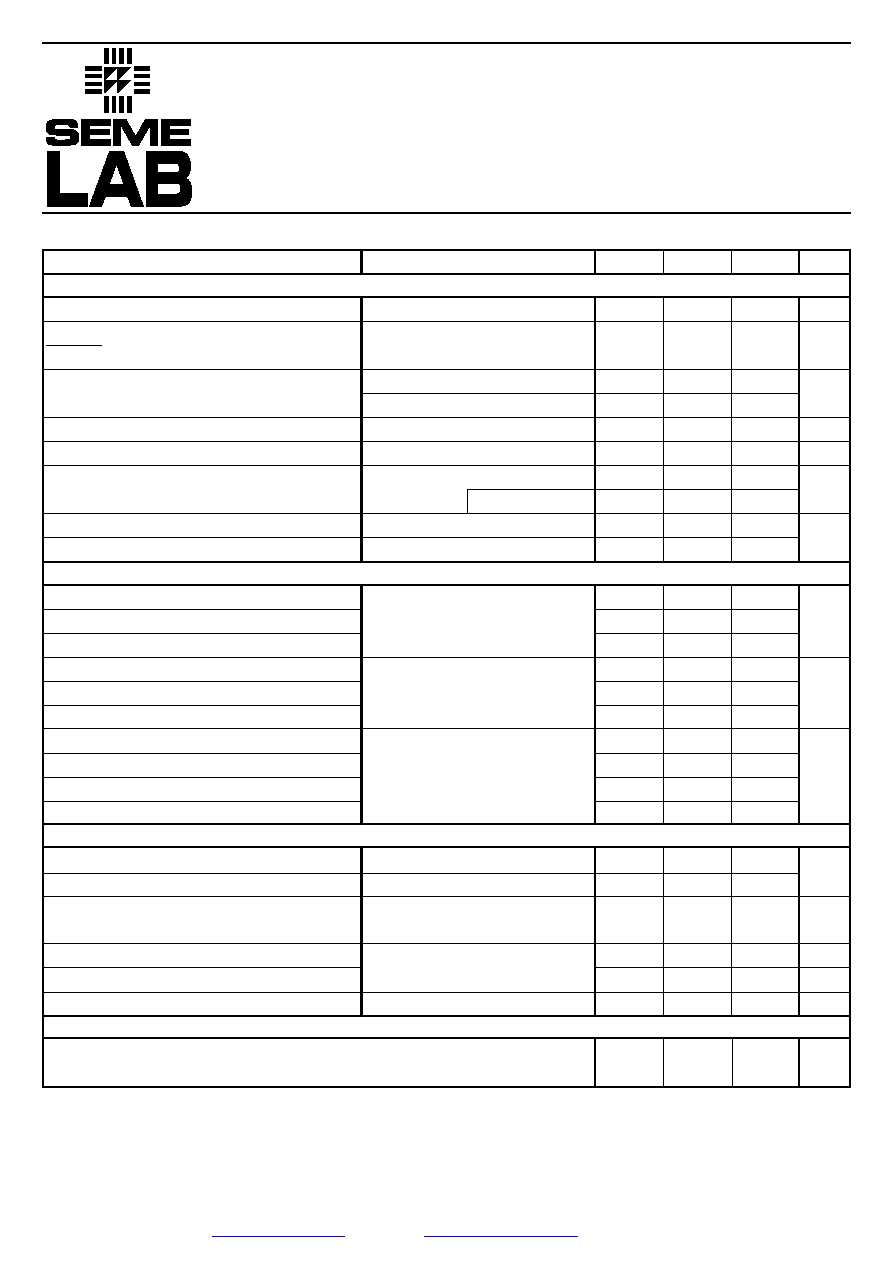
ELECTRICAL CHARACTERISTICS (T
J = 25°C unless otherwise stated)
Drain – Source Breakdown Voltage
Temperature Coefficient of
Breakdown Voltage
Static Drain – Source On–State
Resistance 2
Gate Threshold Voltage
Forward Transconductance 2
Zero Gate Voltage Drain Current
Forward Gate – Source Leakage
Reverse Gate – Source Leakage
Input Capacitance
Output Capacitance
Reverse Transfer Capacitance
Total Gate Charge
Gate – Source Charge
Gate – Drain (“Miller”) Charge
Turn– On Delay Time
Rise Time
Turn–Off Delay Time
Fall Time
Continuous Source Current
Pulse Source Current 1
Diode Forward Voltage 2
Reverse Recovery Time 2
Reverse Recovery Charge 2
Forward Turn–On Time
200
0.29
0.18
0.25
2.0
4.0
6.1
25
250
100
–100
1300
400
130
60
10.6
37.6
20
105
58
67
18
72
1.5
500
5.3
Negligible
4.0
V
V/ °C
V
S(
A
nA
pF
nC
ns
A
V
ns
C
nH
BVDSS
BV
DSS
T
J
RDS(on)
VGS(th)
gfs
IDSS
IGSS
Ciss
Coss
Crss
Qg
Qgs
Qgd
td(on)
tr
td(off)
tf
IS
ISM
VSD
trr
Qrr
ton
LD
LS
STATIC ELECTRICAL RATINGS
1) Repetitive Rating – Pulse width limited by Maximum Junction Temperature
2) Pulse Test: Pulse Width
≤ 300s, δ≤ 2%.
DYNAMIC CHARACTERISTICS
SOURCE – DRAIN DIODE CHARACTERISTICS
Internal Drain Inductance Measured from drain lead (6mm / 0.25in from package) to
Internal Source Inductance source lead (6mm / 0.25in from package).
PACKAGE CHARACTERISTICS
(
)
相關(guān)PDF資料 |
PDF描述 |
|---|---|
| 2N721 | 35 V, PNP, Si, SMALL SIGNAL TRANSISTOR, TO-18 |
| 2N722 | 35 V, PNP, Si, SMALL SIGNAL TRANSISTOR, TO-18 |
| 2N722.MOD | 35 V, NPN, Si, SMALL SIGNAL TRANSISTOR, TO-206AA |
| 2N722S | 35 V, NPN, Si, SMALL SIGNAL TRANSISTOR, TO-206AA |
| 2N7221 | 10 A, 400 V, 0.7 ohm, N-CHANNEL, Si, POWER, MOSFET, TO-254AA |
相關(guān)代理商/技術(shù)參數(shù) |
參數(shù)描述 |
|---|---|
| 2N7219UJANTX | 制造商:International Rectifier 功能描述:Trans MOSFET N-CH 200V 18A 3-Pin SMD-1 |
| 2N7219UJANTXV | 制造商:International Rectifier 功能描述: |
| 2N721A | 制造商:未知廠家 制造商全稱:未知廠家 功能描述:TRANSISTOR | BJT | PNP | 35V V(BR)CEO | TO-18 |
| 2N722 | 制造商:SEME-LAB 制造商全稱:Seme LAB 功能描述:Bipolar NPN Device in a Hermetically sealed TO18 Metal Package |
| 2N7221 | 制造商:Microsemi Corporation 功能描述:TRANS MOSFET N-CH 10A 3PIN TO-254 - Bulk |
發(fā)布緊急采購(gòu),3分鐘左右您將得到回復(fù)。