- 您現(xiàn)在的位置:買賣IC網(wǎng) > PDF目錄30545 > 2SC3915 (SANYO SEMICONDUCTOR CO LTD) 500 mA, 50 V, NPN, Si, SMALL SIGNAL TRANSISTOR, TO-236 PDF資料下載
參數(shù)資料
| 型號: | 2SC3915 |
| 廠商: | SANYO SEMICONDUCTOR CO LTD |
| 元件分類: | 小信號晶體管 |
| 英文描述: | 500 mA, 50 V, NPN, Si, SMALL SIGNAL TRANSISTOR, TO-236 |
| 封裝: | CP, 3 PIN |
| 文件頁數(shù): | 1/3頁 |
| 文件大小: | 30K |
| 代理商: | 2SC3915 |
53002RM (KT)/71598HA (KT)/4107TA, TS No.2166-1/3
Any and all SANYO products described or contained herein do not have specifications that can handle
applications that require extremely high levels of reliability, such as life-support systems, aircraft’s
control systems, or other applications whose failure can be reasonably expected to result in serious
physical and/or material damage. Consult with your SANYO representative nearest you before using
any SANYO products described or contained herein in such applications.
SANYO assumes no responsibility for equipment failures that result from using products at values that
exceed, even momentarily, rated values (such as maximum ratings, operating condition ranges,or other
parameters) listed in products specifications of any and all SANYO products described or contained
herein.
PNP/NPN Epitaxial Planar Silicon Transistors
Switching Applications (with Bias Resistance)
Ordering number:ENN2166A
2SA1521/2SC3915
SANYO Electric Co.,Ltd. Semiconductor Company
TOKYO OFFICE Tokyo Bldg., 1-10, 1 Chome, Ueno, Taito-ku, TOKYO, 110-8534 JAPAN
( ) : 2SA1521
Specifications
Absolute Maximum Ratings at Ta = 25C
0.4
0.95 0.95
1.9
2.9
0.5
1.5
2.5
0.5
0.16
0 to 0.1
0.8
1.1
2
3
1
Electrical Characteristics at Ta = 25C
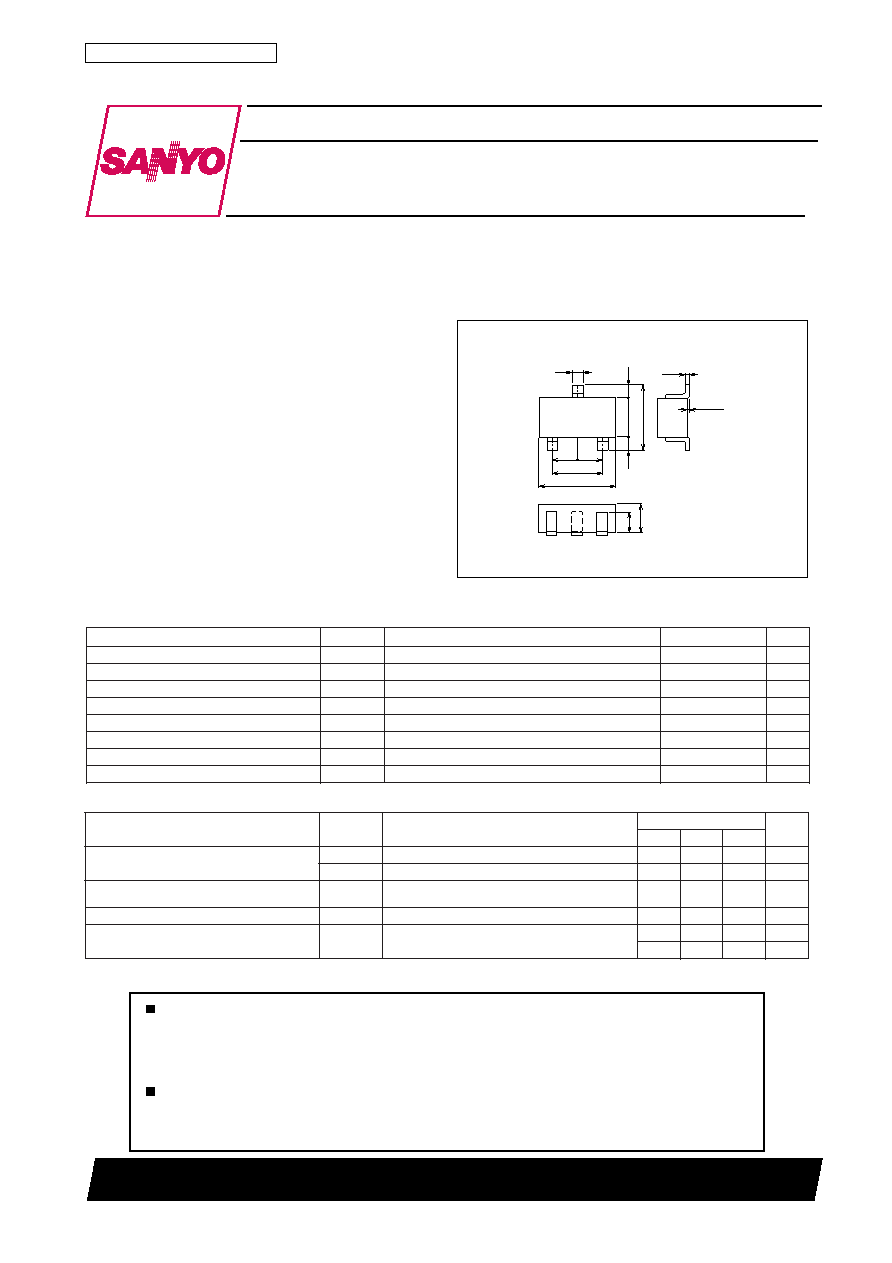
Package Dimensions
unit:mm
2018B
[2SA1521/2SC3915]
Applications
Swicthing circuits, inverter circuits, interface circuits,
dirver circuits.
Features
On-chip bias resistance : R1=2.2k
, R2=2.2k.
Small-sized package : CP.
Large current capacity : IC=500mA.
C
r
e
t
e
m
a
r
a
Pl
o
b
m
y
Ss
n
o
i
t
i
d
n
o
Cs
g
n
i
t
a
Rt
i
n
U
e
g
a
t
l
o
V
e
s
a
B
-
o
t
-
r
o
t
c
e
ll
o
CV
O
B
C
0
5
)
–
(V
e
g
a
t
l
o
V
r
e
t
i
m
E
-
o
t
-
r
o
t
c
e
ll
o
CV
O
E
C
0
5
)
–
(V
e
g
a
t
l
o
V
e
s
a
B
-
o
t
-
r
e
t
i
m
EV
O
B
E
6
)
–
(V
t
n
e
r
u
C
r
o
t
c
e
ll
o
CIC
0
5
)
–
(A
m
)
e
s
l
u
P
(
t
n
e
r
u
C
r
o
t
c
e
ll
o
CI P
C
0
8
)
–
(A
m
n
o
i
t
a
p
i
s
i
D
r
o
t
c
e
ll
o
CPC
0
2W
m
e
r
u
t
a
r
e
p
m
e
T
n
o
i
t
c
n
u
Jj
T
0
5
1
e
r
u
t
a
r
e
p
m
e
T
e
g
a
r
o
t
Sg
t
s
T
0
5
1
+
o
t
5
–
C
r
e
t
e
m
a
r
a
Pl
o
b
m
y
Ss
n
o
i
t
i
d
n
o
C
s
g
n
i
t
a
R
t
i
n
U
n
i
mp
y
tx
a
m
t
n
e
r
u
C
f
o
t
u
C
r
o
t
c
e
ll
o
C
I
O
B
C
V B
C
I
,
V
0
4
)
–
(
=
E 0
=1
.
0
)
–
(A
I
O
E
C
V E
C
I
,
V
0
4
)
–
(
=
B 0
=5
.
0
)
–
(A
t
n
e
r
u
C
f
o
t
u
C
r
e
t
i
m
EI
O
B
E
V B
E
I
,
V
5
)
–
(
=
C 0
=0
6
8
)
–
(
)
–
(
0
4
1
)
–
(
0
7
6
1
A
n
i
a
G
t
n
e
r
u
C
Dh E
F
V E
C
I
,
V
5
)
–
(
=
C
A
m
0
5
)
–
(
=0
5
t
c
u
d
o
r
P
h
t
d
i
w
d
n
a
B
-
n
i
a
GfT
V E
C
I
,
V
0
1
)
–
(
=
C
A
m
5
)
–
(
=
0
5
2z
H
M
)
0
2
(z
H
M
1 : Base
2 : Emitter
3 : Collector
SANYO : CP
Marking 2SA1521 : OL, 2SC3915 ; WY
Continued on next page.
相關PDF資料 |
PDF描述 |
|---|---|
| 2SA1521 | 500 mA, 50 V, PNP, Si, SMALL SIGNAL TRANSISTOR, TO-236 |
| 2SC3929G | 50 mA, 55 V, NPN, Si, SMALL SIGNAL TRANSISTOR |
| 2SC3929G-R | 50 mA, 55 V, NPN, Si, SMALL SIGNAL TRANSISTOR |
| 2SC3929G-T | 50 mA, 55 V, NPN, Si, SMALL SIGNAL TRANSISTOR |
| 2SC3930B | 30 mA, 20 V, NPN, Si, SMALL SIGNAL TRANSISTOR |
相關代理商/技術參數(shù) |
參數(shù)描述 |
|---|---|
| 2SC3915-TB-E | 制造商:SANYO Semiconductor Co Ltd 功能描述:TRANS NPN +RESIS 50V 0.5A SOT23 |
| 2SC3917-AC | 制造商:SANYO Semiconductor Co Ltd 功能描述:TRANS NPN +RES 50V 0.5A SPA |
| 2SC3920 | 制造商:Distributed By MCM 功能描述:SUB ONLY TRANSISTOR TO-9250V .5A .6W ECB |
| 2SC3920-AA | 制造商:SANYO Semiconductor Co Ltd 功能描述:TRANS NPN +RESIS 50V 0.5A TO-92 |
| 2SC3921 | 制造商:Distributed By MCM 功能描述:SUB ONLY SANYO TRANSISTORTO-92 50V .5A .6W ECB |
發(fā)布緊急采購,3分鐘左右您將得到回復。