- 您現(xiàn)在的位置:買賣IC網(wǎng) > PDF目錄33490 > 2SK2554-E 75 A, 60 V, 0.01 ohm, N-CHANNEL, Si, POWER, MOSFET PDF資料下載
參數(shù)資料
| 型號(hào): | 2SK2554-E |
| 元件分類: | JFETs |
| 英文描述: | 75 A, 60 V, 0.01 ohm, N-CHANNEL, Si, POWER, MOSFET |
| 封裝: | SC-65, TO-3P, 3 PIN |
| 文件頁(yè)數(shù): | 1/4頁(yè) |
| 文件大小: | 103K |
| 代理商: | 2SK2554-E |
1998
Document No. D16160EJ1V0DS00 (1st edition)
Date Published April 2002 N CP(K)
Printed in Japan
COMPOUND TRANSISTOR
AA1A4Z
on-chip resistor NPN silicon epitaxial transistor
For mid-speed switching
DATA SHEET
2002
The information in this document is subject to change without notice. Before using this document, please
confirm that this is the latest version.
Not all devices/types available in every country. Please check with local NEC representative for
availability and additional information.
FEATURES
On-chip bias resistor
(R1 = 10 k
)
Complementary transistor with AN1A4Z
ABSOLUTE MAXIMUM RATINGS (Ta = 25
°°°°C)
Parameter
Symbol
Ratings
Unit
Collector to base voltage
VCBO
60
V
Collector to emitter voltage
VCEO
50
V
Emitter to base voltage
VEBO
5V
Collector current (DC)
IC(DC)
100
mA
Collector current (Pulse)
IC(pulse) *
200
mA
Total power dissipation
PT
250
mW
Junction temperature
Tj
150
°C
Storage temperature
Tstg
55 to +150
°C
*PW
≤ 10 ms, duty cycle ≤ 50 %
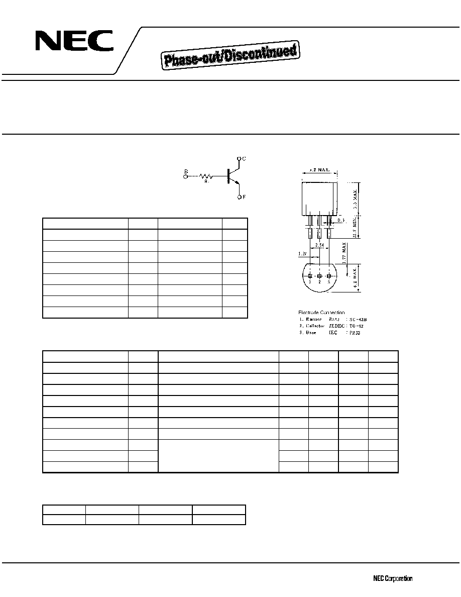
PACKAGE DRAWING (UNIT: mm)
ELECTRICAL CHARACTERISTICS (Ta = 25
°°°°C)
Parameter
Symbol
Conditions
MIN.
TYP.
MAX.
Unit
Collector cutoff current
ICBO
VCB = 50 V, IE = 0
100
nA
DC current gain
hFE1 **
VCE = 5.0 V, IC = 5.0 mA
135
340
600
DC current gain
hFE2 **
VCE = 5.0 V, IC = 50 mA
100
300
Collector saturation voltage
VCE(sat) **
IC = 5.0 mA, IB = 0.25 mA
0.04
0.2
V
Low level input voltage
VIL **
VCE = 5.0 V, IC = 100
A
0.55
0.5
V
High level input voltage
VIH **
VCE = 0.2 V, IC = 5.0 mA
2.0
0.8
V
Input resistance
R1
7.0
10
13.0
k
Turn-on time
ton
0.2
s
Storage time
tstg
5.0
s
Turn-off time
toff
VCC = 5.0 V, RL = 1.0 k
VI = 5.0 V, PW = 2.0
s
duty cycle
≤2 %
6.0
s
** Pulse test PW
≤ 350
s, duty cycle ≤ 2 %
hFE CLASSIFICATION
Marking
Q
P
K
hFE1
135 to 270
200 to 400
300 to 600
相關(guān)PDF資料 |
PDF描述 |
|---|---|
| 2SK2554 | 0.01 ohm, POWER, FET |
| 2SK2554 | 75 A, 60 V, 0.01 ohm, N-CHANNEL, Si, POWER, MOSFET |
| 2SK2555TP-FA | 12000 mA, 30 V, N-CHANNEL, Si, SMALL SIGNAL, MOSFET |
| 2SK2557 | 7 A, 30 V, 0.06 ohm, N-CHANNEL, Si, POWER, MOSFET |
| 2SK2442 | 7 A, 30 V, 0.048 ohm, N-CHANNEL, Si, POWER, MOSFET |
相關(guān)代理商/技術(shù)參數(shù) |
參數(shù)描述 |
|---|---|
| 2SK2555 | 制造商:未知廠家 制造商全稱:未知廠家 功能描述: |
| 2SK2556 | 制造商:未知廠家 制造商全稱:未知廠家 功能描述: |
| 2SK2557 | 制造商:未知廠家 制造商全稱:未知廠家 功能描述: |
| 2SK2559 | 制造商:SHINDENGEN 制造商全稱:Shindengen Electric Mfg.Co.Ltd 功能描述:VZ Series Power MOSFET(200V 10A) |
| 2SK2559-7100 | 制造商:Shindengen Electric Mfg 功能描述:Cut Tape |
發(fā)布緊急采購(gòu),3分鐘左右您將得到回復(fù)。