- 您現(xiàn)在的位置:買賣IC網(wǎng) > PDF目錄293797 > 3650MG Optically-Coupled Linear ISOLATION AMPLIFIERS PDF資料下載
參數(shù)資料
| 型號: | 3650MG |
| 元件分類: | 隔離放大器 |
| 英文描述: | Optically-Coupled Linear ISOLATION AMPLIFIERS |
| 中文描述: | 光耦合線性隔離放大器 |
| 文件頁數(shù): | 11/13頁 |
| 文件大小: | 127K |
| 代理商: | 3650MG |

7
3650/52
function of the accuracy of the matching and is further
enhanced by the use of negative feedback in the input stage.
Advanced laser trimming techniques are used to further
compensate for residual matching errors.
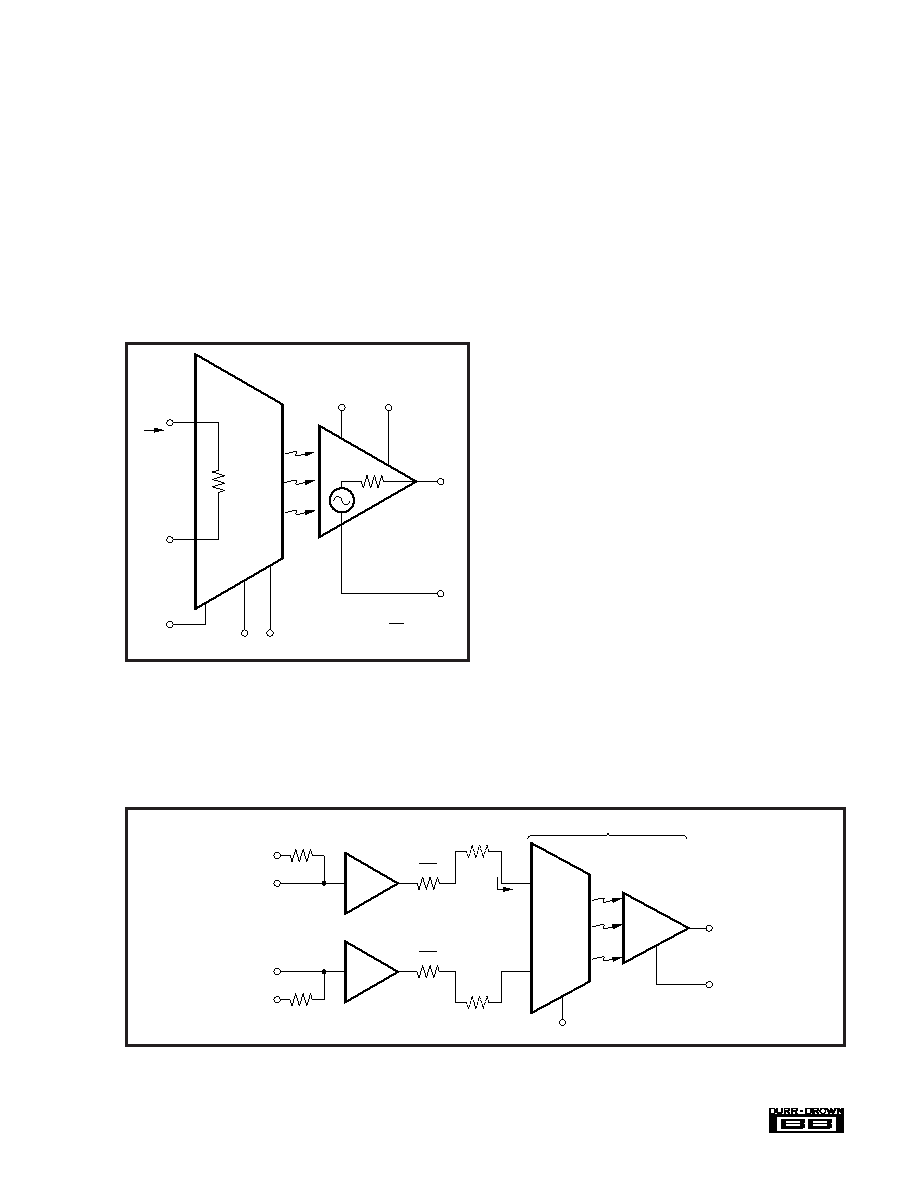
A model of the 3650 suitable for simple circuit analysis is
shown in Figure 3. The output is a current dependent voltage
source, VD, whose value depends on the input current. Thus,
the 3650 is a transconductance amplifier with a gain of one
volt per microamp. When voltage sources are used, the input
current is derived by using gain setting resistors in series
with the voltage source (see Installation and Operating
Instructions for details). RIN is the differential input imped-
ance. The common-mode and isolation impedances are very
high and are assumed to be infinite for this model.
FIGURE 3. Simple Model of 3650.
A simplified model of the 3652 is shown in Figure 4. The
isolation and output stages are identical to the 3650. Addi-
tional input circuitry consisting of FET buffer amplifiers and
input protection resistors have been added to give higher
differential and common-mode input impedance (1011
),
lower bias currents (50pA) and overvoltage protection. The
+IR and –IR inputs have a 10ms pulse rating of 6000V
differential and 3000V common-mode (see Definitions for a
discussion of common-mode and isolation-mode voltages.)
The addition of the buffer amplifiers also creates a voltage-
in voltage-out transfer function with the gain set by RG1 and
RG2.
INSTALLATION AND
OPERATING INSTRUCTIONS
POWER SUPPLY CONNECTIONS
The power supply connections for the 3650 and 3652 are
shown in Figure 5. When a DC/DC converter is used for
isolated power, it is placed in parallel with the isolation
barrier of the amplifier. This can lower the isolation imped-
ance and degrade the isolation-mode rejection of the overall
circuit. Therefore, a high quality, low leakage DC/DC con-
verter such as the Burr-Brown Model 722 should be used.
OFFSET VOLTAGE ADJUSTMENTS
The offset nulling circuits are identical for the 3650 and
3652 and are shown in Figure 5. The offset adjust circuitry
is optional and the units will meet the stated specifications
with the BAL terminals unconnected. Provisions are avail-
able to null both the input and output stage offsets. If the
amplifier is operated at a fixed gain, normally only one
adjustment will be used: the output stage (10k
adjustment)
for low gains and the input stage (50k
adjustment) for high
gains, (
>10).
Use the following procedure if it is desired to null both input
and output components. (For example, if the gain of the
amplifier is to be switched). The input stage offset is first
nulled (50k
adjustment) with the appropriate input signal
pins connected to input common and the amplifier set at its
maximum gain. The gain is then set to its minimum value
and the output offset is nulled (10k
adjustment).
FIGURE 4. Simple Model of 3652.
(Output)
+
R
IN
+
–
23
10
11
I
IN
(Input)
C
12
14
13
+V
–V
R
OUT
V
D
–
17
+V
CC
–V
CC
26
20
V
D = IIN X
1V
A
C
R
G1
R
G2
11
10
C
(Output)
23
C (Input)
A
1
A
2
R
O
2
R
O
2
8
9
–I
R
+I
R
+I
–I
I
IN
Same as 3650 in Figure 3.
1.6M
1.6M
17
6
4
3
1
12
相關(guān)PDF資料 |
PDF描述 |
|---|---|
| 3650MGHG | Optically-Coupled Linear ISOLATION AMPLIFIERS |
| 3650MGHG1 | Optically-Coupled Linear ISOLATION AMPLIFIERS |
| 3650 | Optically-Coupled Linear ISOLATION AMPLIFIERS |
| 3652HG | Optically-Coupled Linear ISOLATION AMPLIFIERS |
| 3652JG | BOARD ADD-ON DUAL PIXEL LVDS PNL |
相關(guān)代理商/技術(shù)參數(shù) |
參數(shù)描述 |
|---|---|
| 3650MGHG | 制造商:BB 制造商全稱:BB 功能描述:Optically-Coupled Linear ISOLATION AMPLIFIERS |
| 3650MGHG1 | 制造商:BB 制造商全稱:BB 功能描述:Optically-Coupled Linear ISOLATION AMPLIFIERS |
| 3650S-1-102 | 制造商:Bourns Inc 功能描述: |
| 3650S-1-103 | 制造商:Bourns Inc 功能描述:Res POT 10K Ohm 3% 2.5W 10(Elec)/10(Mech)Turn (44.45 X 62.74mm) J-Hook Panel Mount |
| 3650S-1-104 | 制造商:Bourns Inc 功能描述: |
發(fā)布緊急采購,3分鐘左右您將得到回復(fù)。