- 您現(xiàn)在的位置:買賣IC網(wǎng) > PDF目錄298320 > 3D7523 (Data Delay Devices, Inc.) MONOLITHIC MANCHESTER ENCODER/DECODER PDF資料下載
參數(shù)資料
| 型號: | 3D7523 |
| 廠商: | Data Delay Devices, Inc. |
| 英文描述: | MONOLITHIC MANCHESTER ENCODER/DECODER |
| 中文描述: | 整體式曼徹斯特編碼/解碼器 |
| 文件頁數(shù): | 3/5頁 |
| 文件大小: | 164K |
| 代理商: | 3D7523 |

3D7523
APPLICATION NOTES (CONT’D)
DECODER
to one over twice the baud rate. Otherwise, the
input is presented at the clock output unchanged,
shifted in time. Therefore, the clock duty cycle is
strongly dependent on the baud rate, as this will
affect the clock-high duration.
The Manchester decoder subsystem samples the
input at precise pre-selected intervals to retrieve
the data and to recover the clock from the
received data stream. Its architecture comprises
finely tuned delay elements and proprietary
circuitry which, in conjunction with other circuits,
implement the data decoding and clock recovery
function.
The clock output falling edge is not operated on
by the clock recovery circuitry. It, therefore,
preserves more accurately the clock frequency
information embedded in the transmitted data. It
can therefore be used, if desired, to retrieve clock
frequency information.
Typically, the encoded data transmitted from a
source arrives at the decoder corrupted. Such
corruption of the received data manifests itself as
jitter and/or pulse width distortion at the decoder
input. The instantaneous deviations from
nominal Baud Rate and/or Pulse Width (high or
low) adversely impact the data extraction and
clock recovery function if their published limits
are exceeded. See Table 4, Allowed Baud
Rate/Duty Cycle. The decoder, being a self-
timed device, is tolerant of frequency modulation
(jitter) present in the input data stream, provided
that the input data pulse width variations remain
within the allowable ranges.
INPUT SIGNAL CHARACTERISTICS
The 3D7523 inputs are TTL compatible. The
user should assure him/herself that the 1.5
volt TTL threshold is used when referring to all
timing, especially to the input clock duty cycle
(encoder) and the received data (decoder).
POWER SUPPLY AND
TEMPERATURE CONSIDERATIONS
CMOS integrated circuitry is strongly dependent
on power supply and temperature. The
monolithic 3D7523 Manchester encoder/decoder
utilizes novel and innovative compensation
circuitry to minimize timing variations induced by
fluctuations in power supply and/or temperature.
Nevertheless, optimum performance is achieved
by providing a stable power supply and a clean
ground plane, and by placing a bypass capacitor
(0.1uf typically) as close to the device as
possible.
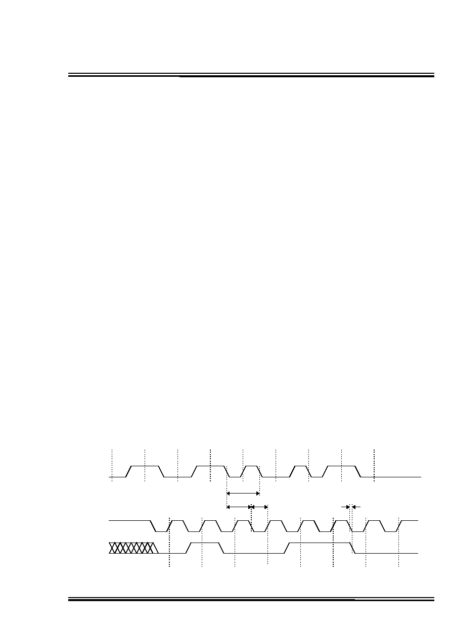
The decoder presents at its outputs the decoded
data (inverted) and the recovered clock. The
decoded data is valid at the rising edge of the
clock.
The clock recovery function operates in two
modes dictated by the input data stream bit
sequence. When a data bit is succeeded by its
inverse, the clock recovery circuit is engaged and
forces the clock output low for a time equal
CLOCK
(CLK)
RECEIVED
(RX)
Figure 2: Timing Diagram (Decoder)
tC
DECODED
1011001
ENCODED
1011001
0
DATA
(DATB)
tCL
tCWL
tCD
Doc #06003
DATA DELAY DEVICES, INC.
3
5/8/2006
3 Mt. Prospect Ave. Clifton, NJ 07013
相關(guān)PDF資料 |
PDF描述 |
|---|---|
| 3EZ120D5 | surface mount silicon Zener diodes |
| 3EZ130D5 | CAP 1200UF 200V ELECT TS-HB |
| 3EZ150D5 | surface mount silicon Zener diodes |
| 3EZ160D5 | CAP 2200UF 6.3V ELECT FC RADIAL |
| 3EZ16D5 | surface mount silicon Zener diodes |
相關(guān)代理商/技術(shù)參數(shù) |
參數(shù)描述 |
|---|---|
| 3D7523-0.5 | 制造商:DATADELAY 制造商全稱:Data Delay Devices, Inc. 功能描述:MONOLITHIC MANCHESTER ENCODER/DECODER |
| 3D7523-1 | 制造商:DATADELAY 制造商全稱:Data Delay Devices, Inc. 功能描述:MONOLITHIC MANCHESTER ENCODER/DECODER |
| 3D7523-10 | 制造商:DATADELAY 制造商全稱:Data Delay Devices, Inc. 功能描述:MONOLITHIC MANCHESTER ENCODER/DECODER |
| 3D7523-20 | 制造商:DATADELAY 制造商全稱:Data Delay Devices, Inc. 功能描述:MONOLITHIC MANCHESTER ENCODER/DECODER |
| 3D7523-25 | 制造商:DATADELAY 制造商全稱:Data Delay Devices, Inc. 功能描述:MONOLITHIC MANCHESTER ENCODER/DECODER |
發(fā)布緊急采購,3分鐘左右您將得到回復(fù)。