- 您現(xiàn)在的位置:買賣IC網(wǎng) > PDF目錄33563 > 4016BM (National Semiconductor Corporation) Quad Bilateral Switch PDF資料下載
參數(shù)資料
| 型號(hào): | 4016BM |
| 廠商: | National Semiconductor Corporation |
| 英文描述: | Quad Bilateral Switch |
| 中文描述: | 四雙邊開關(guān) |
| 文件頁(yè)數(shù): | 4/8頁(yè) |
| 文件大?。?/td> | 168K |
| 代理商: | 4016BM |

AC Electrical Characteristics (Continued)
TAe25 C tretfe20 ns and VSSe0V unless otherwise specified
Symbol
Parameter
Conditions
Min
Typ
Max
Units
Frequency Response
Switch
VCeVDDe5V VSSeb5V
40
MHz
‘‘ON’’ (Frequency at b3 dB)
RLe1kX VISe5VP-P
20 Log10 VOS VOS (1 kHz) bdB
(
Figure 4 )
Feedthrough
Switch ‘‘OFF’’
VDDe5V VCeVSSeb5V
125
MHz
(Frequency at b50 dB)
RLe1kX VISe5VP-P
20 Log10 (VOS VIS)eb50 dB
(
Figure 4 )
Crosstalk Between Any Two
VDDeVC(A)e5V VSSeVC(B)eb5V
09
MHz
Switches (Frequency at b50 dB)
RLe1kXVIS(A)e5VP-P
20 Log10 (VOS(B) VOS(A) )eb50 dB
(
Figure 5 )
Crosstalk Control Input to
VDDe10V RLe10 kX
150
mVP-P
Signal Output
RINe1kX VCCe10V Square Wave
CLe50 pF (Figure 6 )
Maximum Control Input
RLe 1kX CLe50 pF (Figure 7 )
VOS(f)e
VOS(1 kHz)
VDDe5V
65
MHz
VDDe10V
80
MHz
VDDe15V
90
MHz
CIS
Signal Input Capacitance
4
pF
COS
Signal Output Capacitance
VDDe10V
4
pF
CIOS
Feedthrough Capacitance
VCe0V
02
pF
CIN
Control Input Capacitance
5
75
pF
AC Paramters are guaranteed by DC correlated testing
Note 1
‘‘Absolute Maximum Ratings’’ are those values beyond which the safety of the device cannot be guaranteed They are not meant to imply that the devices
should be operated at these limits The tables of ‘‘Recommended Operating Conditions’’ and ‘‘Electrical Characteristics’’ provide conditions for actual device
operation
Note 2
VSSe0V unless otherwise specified
Note 3
These devices should not be connected to circuits with the power ‘‘ON’’
Note 4
In all cases there is approximately 5 pF of probe and jig capacitance on the output however this capacitance is included in CL wherever it is specified
Note 5
VIS is the voltage at the inout pin and VOS is the voltage at the outin pin VC is the voltage at the control input
Note 6
If the switch input is held at VDD VIHC is the control input level that will cause the switch output to meet the standard ‘‘B’’ series VOH and IOH output levels
If the analog switch input is connected to VSS VIHC is the control input level
which allows the switch to
sink standard ‘‘B’’ series
lIOHl high level current and still
maintain a VOL s ‘‘B’’ series These currents are shown in Figure 8
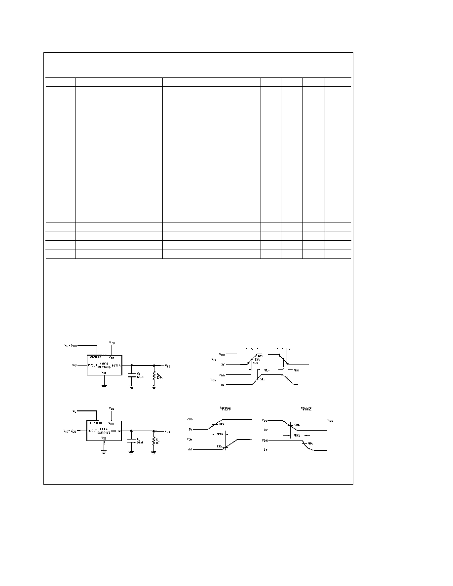
AC Test Circuits and Switching Time Waveforms
Figure 1 tPLH tPLH Propagation Delay Time Signal Input to Signal Output
TLF5661 – 2
FIGURE 2 tPZH tPHZ Propagation Delay Time Control to Signal Output
4
相關(guān)PDF資料 |
PDF描述 |
|---|---|
| 401CMQ045 | SCHOTTKY RECTIFIER |
| 401CMQ | SCHOTTKY RECTIFIER |
| 401CMQ035 | SCHOTTKY RECTIFIER |
| 401CMQ040 | SCHOTTKY RECTIFIER |
| 401CNQ035 | CONN MINI-D RIBBON 1AA |
相關(guān)代理商/技術(shù)參數(shù) |
參數(shù)描述 |
|---|---|
| 4016-BOX | 功能描述:LED DVR CTLR QUADPUCK 4CH BOX RoHS:是 類別:電源 - 外部/內(nèi)部(非板載) >> 配件 系列:4016 QuadPuck 標(biāo)準(zhǔn)包裝:1 系列:VS/MP 附件類型:連接器套件 適用于相關(guān)產(chǎn)品:- |
| 4016BPC | 制造商:Freescale Semiconductor 功能描述: |
| 4016GB | 制造商:Greenlee Textron Inc 功能描述:OIL-HYDRAULIC 1 GAL |
| 4016-GX | 制造商:FLORIDA MISC. 功能描述: 制造商:Florida Misc. 功能描述: |
| 40-16-LF-S | 制造商:Birtcher Products 功能描述: |
發(fā)布緊急采購(gòu),3分鐘左右您將得到回復(fù)。