- 您現(xiàn)在的位置:買(mǎi)賣(mài)IC網(wǎng) > PDF目錄33624 > 407T21J060M0010 (CTS CORP) QUARTZ CRYSTAL RESONATOR, 60.001 MHz PDF資料下載
參數(shù)資料
| 型號(hào): | 407T21J060M0010 |
| 廠商: | CTS CORP |
| 元件分類: | 晶體 |
| 英文描述: | QUARTZ CRYSTAL RESONATOR, 60.001 MHz |
| 封裝: | GREEN COMPLIANT, CERAMIC, METAL-4 |
| 文件頁(yè)數(shù): | 2/3頁(yè) |
| 文件大小: | 213K |
| 代理商: | 407T21J060M0010 |

Document No. 008-0261-0
Page 2 - 3
Rev. G
CTS Electronic Components, Inc. 171 Covington Drive Bloomingdale, IL 60108
Model 407
7.0x5.0mm Low Cost
Surface Mount Crystal
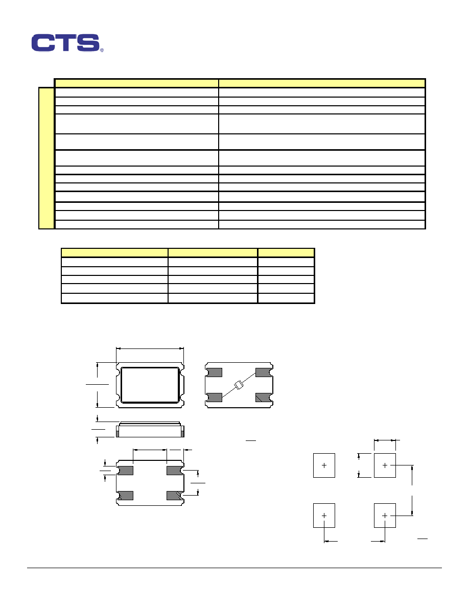
ELECTRICAL CHARACTERISTICS
PARAMETER
VALUE
Operating Mode (Note 1)
Fundamental or 3RD Overtone
Crystal Cut
AT-Cut
Frequency Range
6.0 MHz to 156.25 MHz
± 30 ppm Standard
(± 10 ppm, ±15 ppm and ± 20 ppm Available)
Frequency Stability Tolerance
± 50 ppm Standard
(Operating Temperature Range, Referenced to 25°C Reading)
(± 10 ppm, ±15 ppm, ± 20 ppm, ± 30 ppm and ± 40 ppm Available)
-20°C to +70°C Standard
(-40°C to +85°C Available)
Storage Temperature Range
-55°C to +125°C
Equivalent Series Resistance
See ESR Table
Load Capacitance or Resonance Mode
See Ordering Information
Shunt Capacitance (C0)
7.0 pF Maximum
Drive Level
25 W Typical, 100 W Maximum
Aging @ 25°C
± 3 ppm/year maximum
Reflow Condition, per JEDEC J-STD-020
+255°C ± 5°C, 10 Seconds Maximum
El
ec
tr
ic
al
P
ar
am
ete
rs
Frequency Tolerance @ 25°C
Operating Temperature Range
EQUIVALENT SERIES RESISTANCE TABLE
FREQUENCY RANGE
MODE of OSCILLATION ESR Maximum
6.000 MHz - 7.999 MHz
Fundamental
80 Ohms
8.000 MHz - 15.999 MHz
Fundamental
60 Ohms
16.000 MHz - 50.000 MHz
Fundamental
40 Ohms
30.001 MHz - 60.000 MHz
3RD Overtone
100 Ohms
60.001 MHz - 156.25.000 MHz
3RD Overtone
80 Ohms
MECHANICAL SPECIFICATIONS
MARKING INFORMATION
1. ** - Manufacturing Site Code.
2. YYWW – Date Code, YY – Year, WW – Week.
3. XXXMXXXX – Frequency marked with 4
significant digits after the ‘M’.
4. Complete CTS part number, frequency value
and date code information must appear on
reel and box labels.
SUGGESTED SOLDER PAD GEOMETRY
0.252 [6.40]
0.100 [2.54]
0.087 [2.20]
Key:
[mm]
Inch
0.055 [1.40]
12
3
4
PACKAGE DRAWING
0.039
( 1.0 )
1
4
2
3
2
3
1
4
Max
Top View
( 2.54 )
0.100
( 1.2 )
0.047
0.181
( 4.6 )
( 1.30 )
( 7.00 ±0.20 )
0.276 ±0.008
0.051
Key:
( MM )
Inch
( 5.00 ±0.20 )
0.197 ±0.008
Bottom View
Notes:
1. Termination pads (e4), barrier-plating is nickel (Ni) with gold (Au) flash plate.
2. Terminations #2, #4 and the metal lid are connected internally.
End user may connect these pins to circuit ground.
CTS**YYWW
● XXXMXXXX
相關(guān)PDF資料 |
PDF描述 |
|---|---|
| 407F14J015M9990 | QUARTZ CRYSTAL RESONATOR, 15.999 MHz |
| 407F15S006M0000 | QUARTZ CRYSTAL RESONATOR, 6 MHz |
| 407F19B006M0000 | QUARTZ CRYSTAL RESONATOR, 6 MHz |
| 407F19G007M9990 | QUARTZ CRYSTAL RESONATOR, 7.999 MHz |
| 407F16L016M0000 | QUARTZ CRYSTAL RESONATOR, 16 MHz |
相關(guān)代理商/技術(shù)參數(shù) |
參數(shù)描述 |
|---|---|
| 407T21JM | 制造商:CTS 制造商全稱:CTS Corporation 功能描述:Surface Mount Quartz Crystal |
| 407T21KM | 制造商:CTS 制造商全稱:CTS Corporation 功能描述:Surface Mount Quartz Crystal |
| 407T21LM | 制造商:CTS 制造商全稱:CTS Corporation 功能描述:Surface Mount Quartz Crystal |
| 407T21SM | 制造商:CTS 制造商全稱:CTS Corporation 功能描述:Surface Mount Quartz Crystal |
| 407T22AM | 制造商:CTS 制造商全稱:CTS Corporation 功能描述:Surface Mount Quartz Crystal |
發(fā)布緊急采購(gòu),3分鐘左右您將得到回復(fù)。