- 您現(xiàn)在的位置:買賣IC網(wǎng) > PDF目錄371600 > 522955X IC PDF資料下載
參數(shù)資料
| 型號: | 522955X |
| 英文描述: | IC |
| 中文描述: | 集成電路 |
| 文件頁數(shù): | 7/12頁 |
| 文件大小: | 195K |
| 代理商: | 522955X |
7
LT1130A/LT1140A Series
C
HARA TERISTICS
U
A
TYPICAL PERFOR
CE
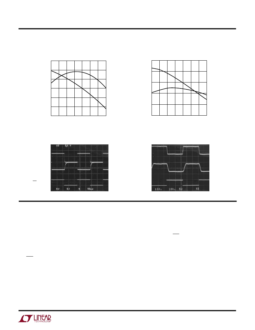
Shutdown to Driver Output
Receiver Short-Circuit Current
Driver Short-Circuit Current
Driver Output Waveforms
LT1137A TPC12
10
5
0
–10
–5
DRIVER OUTPUT
R
= 3k
C
L
= 2500pF
INPUT
DRIVER OUTPUT
R
L
= 3k
PI FU
V
CC
:
5V Input Supply Pin. Supply current drops to zero in
the shutdown mode. This pin should be decoupled with a
0.1
μ
F ceramic capacitor close to the package pin. Insuffi-
cient supply bypassing can result in low output drive levels
and erratic charge pump operation.
GND:
Ground Pin.
ON/OFF:
Control the operation mode of the device and is
TTL/CMOS compatible. A logic low puts the device in the
shutdown mode which reduces input supply curent to zero
and places all of the drivers and receivers in high imped-
ance state. A logic high fully enables the transceiver.
DRIVER DISABLE:
This pin provides an alternate control
for the charge pump and RS232 drivers. A logic high on
this pin shuts down the charge pump and places all drivers
U
in a high impedance state. Receivers remain active under
these conditions. Floating the DRIVER DISABLE pin or
driving it to a logic low level fully enables the transceiver.
A logic low on the ON/OFF pin supersedes the state of the
DRIVER DISABLE pin. Supply current drops to 4mA when
in driver disable mode.
V
+
:
Positive Supply Output (RS232 Drivers). V
+
≈
2V
CC
–
1.5V. This pin requires an external charge storage capaci-
tor C
≥
1.0
μ
F, tied to ground or V
CC
. Larger value capaci-
tors may be used to reduce supply ripple. With multiple
transceivers, the V
+
and V
–
pins may be paralleled into
common capacitors. For large numbers of transceivers,
increasing the size of the shared common storage capaci-
tors is recommended to reduce ripple.
TEMPERATURE (°C)
–55
S
20
25
30
25
75
LT1137A TPC10
15
10
–25
0
50
100
125
5
0
ISC
+
ISC
–
TEMPERATURE (°C)
–55
0
S
20
50
0
50
75
LT1137A TPC11
10
40
30
–25
25
100
125
ISC
+
ISC
–
LT1137A TPC13
DRIVER
OUTPUT HIGH
R
L
= 3k
ON/OFF PIN
DRIVER
OUTPUT LOW
R
L
= 3k
相關PDF資料 |
PDF描述 |
|---|---|
| 508624E | Dual/Triple Ultra-Low-Voltage SOT23 µP Supervisory Circuits |
| 508629F | Dual/Triple Ultra-Low-Voltage SOT23 µP Supervisory Circuits |
| 522975B | Dual/Triple Ultra-Low-Voltage SOT23 µP Supervisory Circuits |
| 508635X | IC |
| 508653F | Dual/Triple Ultra-Low-Voltage SOT23 µP Supervisory Circuits |
相關代理商/技術參數(shù) |
參數(shù)描述 |
|---|---|
| 522956H | 制造商:未知廠家 制造商全稱:未知廠家 功能描述:IC |
| 522957 | 制造商:AMETEK Technical and Industrial Products 功能描述:Motor, 3HP, 3PHm 575, TEFC |
| 522957F | 制造商:未知廠家 制造商全稱:未知廠家 功能描述:IC |
| 522958D | 制造商:未知廠家 制造商全稱:未知廠家 功能描述:IC-ADJ DC/DC CONVERTER |
| 522959B | 制造商:未知廠家 制造商全稱:未知廠家 功能描述:IC-INV DC/DC CONVERTER |
發(fā)布緊急采購,3分鐘左右您將得到回復。