- 您現(xiàn)在的位置:買賣IC網(wǎng) > PDF目錄34248 > 530AB506M000DGR (SILICON LABORATORIES) CRYSTAL OSCILLATOR, CLOCK, 506 MHz, LVPECL OUTPUT PDF資料下載
參數(shù)資料
| 型號(hào): | 530AB506M000DGR |
| 廠商: | SILICON LABORATORIES |
| 元件分類: | XO, clock |
| 英文描述: | CRYSTAL OSCILLATOR, CLOCK, 506 MHz, LVPECL OUTPUT |
| 封裝: | ROHS COMPLIANT, SMD, 6 PIN |
| 文件頁數(shù): | 2/12頁 |
| 文件大小: | 215K |
| 代理商: | 530AB506M000DGR |
Si530/531
10
Rev. 1.1
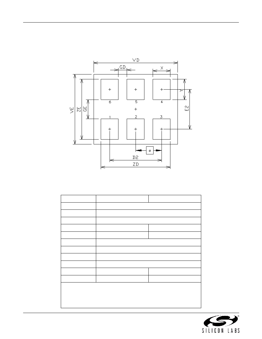
6. 6-Pin PCB Land Pattern
Figure 4 illustrates the 6-pin PCB land pattern for the Si530/531. Table 13 lists the values for the dimensions shown
in the illustration.
Figure 4. Si530/531 PCB Land Pattern
Table 13. PCB Land Pattern Dimensions (mm)
Dimension
Min
Max
D2
5.08 REF
e
2.54 BSC
E2
4.15 REF
GD
0.84
—
GE
2.00
—
VD
8.20 REF
VE
7.30 REF
X1.70 TYP
Y2.15 REF
ZD
—
6.78
ZE
—
6.30
Notes:
1. Dimensioning and tolerancing per the ANSI Y14.5M-1994 specification.
2. Land pattern design based on IPC-7351 guidelines.
3. All dimensions shown are at maximum material condition (MMC).
4. Controlling dimension is in millimeters (mm).
發(fā)布緊急采購,3分鐘左右您將得到回復(fù)。