- 您現(xiàn)在的位置:買賣IC網(wǎng) > PDF目錄114672 > 531AC315M000DGR (SILICON LABORATORIES) CRYSTAL OSCILLATOR, CLOCK, 315 MHz, LVPECL OUTPUT PDF資料下載
參數(shù)資料
| 型號: | 531AC315M000DGR |
| 廠商: | SILICON LABORATORIES |
| 元件分類: | XO, clock |
| 英文描述: | CRYSTAL OSCILLATOR, CLOCK, 315 MHz, LVPECL OUTPUT |
| 封裝: | ROHS COMPLIANT, SMD, 6 PIN |
| 文件頁數(shù): | 11/12頁 |
| 文件大?。?/td> | 215K |
| 代理商: | 531AC315M000DGR |
Si530/531
8
Rev. 1.1
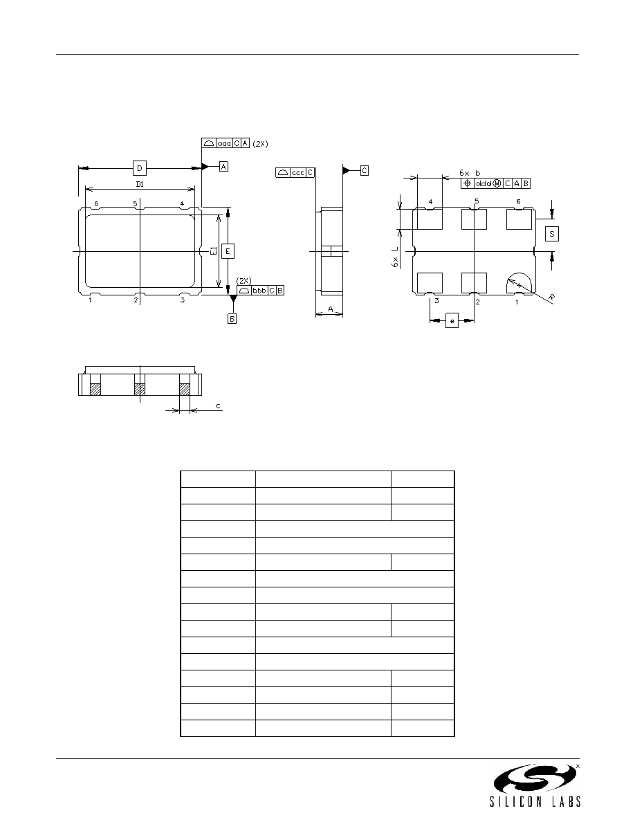
4. Outline Diagram and Suggested Pad Layout
Figure 2 illustrates the package details for the Si530/531. Table 11 lists the values for the dimensions shown in the
illustration.
Figure 2. Si530/531 Outline Diagram
Table 11. Package Diagram Dimensions (mm)
Dimension
Min
Nom
Max
A
1.45
1.65
1.85
b1.2
1.4
1.6
c0.60 TYP.
D
7.00 BSC.
D1
6.10
6.2
6.30
e
2.54 BSC.
E
5.00 BSC.
E1
4.30
4.40
4.50
L
1.07
1.27
1.47
S
1.815 BSC.
R
0.7 REF.
aaa
—
0.15
bbb
—
0.15
ccc
—
0.10
ddd
—
0.10
相關(guān)PDF資料 |
PDF描述 |
|---|---|
| 530HA687M000DGR | CRYSTAL OSCILLATOR, CLOCK, 687 MHz, CMOS/TTL OUTPUT |
| 530HA690M000DGR | CRYSTAL OSCILLATOR, CLOCK, 690 MHz, CMOS/TTL OUTPUT |
| 530HA723M000DG | CRYSTAL OSCILLATOR, CLOCK, 723 MHz, CMOS/TTL OUTPUT |
| 531EC25M0000DGR | CRYSTAL OSCILLATOR, CLOCK, 25 MHz, LVPECL OUTPUT |
| 531MC227M000DG | CRYSTAL OSCILLATOR, CLOCK, 227 MHz, LVPECL OUTPUT |
相關(guān)代理商/技術(shù)參數(shù) |
參數(shù)描述 |
|---|---|
| 531AC500M000DG | 制造商:Silicon Laboratories Inc 功能描述:OSCILLATOR - Trays |
| 531AC500M000DGR | 制造商:Silicon Laboratories Inc 功能描述:OSCILLATOR - Tape and Reel |
| 531AC50M0000DG | 制造商:Silicon Laboratories Inc 功能描述:OSCILLATOR - Trays |
| 531AC50M0000DGR | 制造商:Silicon Laboratories Inc 功能描述:OSCILLATOR - Tape and Reel |
| 531AC622M080DG | 功能描述:標(biāo)準(zhǔn)時鐘振蕩器 SINGLE XO 6PIN 7MMX5MM RoHS:否 制造商:AVX 產(chǎn)品:Standard Clock Oscillators 封裝 / 箱體:7 mm x 5 mm 頻率:75 MHz 頻率穩(wěn)定性:50 PPM 電源電壓:2.5 V 負(fù)載電容: 端接類型:SMD/SMT 最小工作溫度:0 C 最大工作溫度:+ 70 C 輸出格式:LVDS 尺寸: 封裝:Reel 系列: |
發(fā)布緊急采購,3分鐘左右您將得到回復(fù)。