- 您現(xiàn)在的位置:買賣IC網(wǎng) > PDF目錄56721 > 5962-0721301QHX 2 CHANNEL, VIDEO AMPLIFIER, CDFP10 PDF資料下載
參數(shù)資料
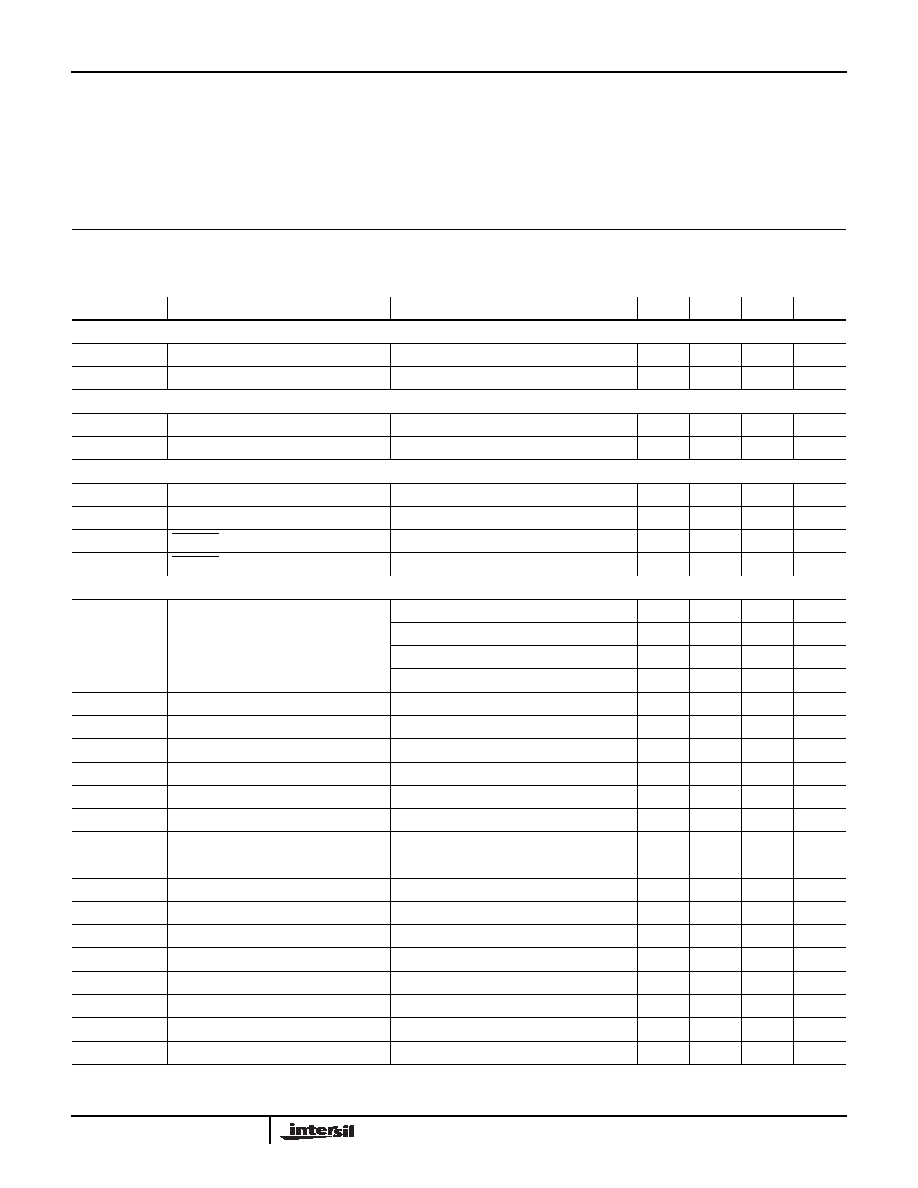
| 型號: | 5962-0721301QHX |
| 元件分類: | 音頻/視頻放大 |
| 英文描述: | 2 CHANNEL, VIDEO AMPLIFIER, CDFP10 |
| 封裝: | CERAMIC, DFP-10 |
| 文件頁數(shù): | 3/6頁 |
| 文件大小: | 133K |
| 代理商: | 5962-0721301QHX |
3
FN6478.0
March 30, 2007
IMPORTANT NOTE: All parameters having Min/Max specifications are guaranteed. Typ values are for information purposes only. Unless otherwise noted, all tests are
at the specified temperature and are pulsed tests, therefore: TJ = TC = TA
Absolute Maximum Ratings (TA = 25°C)
Supply Voltage from VS+ to VS- . . . . . . . . . . . . . . . . . . . . . . . . 5.5V
Input Voltage . . . . . . . . . . . . . . . . . . . . . . . . VS+ +0.3V to VS- -0.3V
Differential Input Voltage . . . . . . . . . . . . . . . . . . . . . . . . . . . . . . . .2V
Continuous Output Current . . . . . . . . . . . . . . . . . . . 20mA / Op Amp
Power Dissipation . . . . . . . . . . . . . . . . . . . . . . . . 74.3mW / Op Amp
Storage Temperature . . . . . . . . . . . . . . . . . . . . . . . . -65°C to +150°C
Ambient Operating Temperature . . . . . . . . . . . . . . . -55°C to +125°C
Operating Junction Temperature . . . . . . . . . . . . . . . . . . . . . . +150°C
CAUTION: Stresses above those listed in “Absolute Maximum Ratings” may cause permanent damage to the device. This is a stress only rating and operation of the
device at these or any other conditions above those indicated in the operational sections of this specification is not implied.
Electrical Specifications
VS+ = 5V, VS- = GND, TA = 25°C, VCM = 2.5V, RL to 2.5V, AV = 1, Unless Otherwise Specified
PARAMETER
DESCRIPTION
CONDITIONS
MIN
TYP
MAX
UNIT
INPUT CHARACTERISTICS
RIN
Input Resistance
Common Mode
3.5
M
Ω
CIN
Input Capacitance
0.5
pF
OUTPUT CHARACTERISTICS
ROUT
Output Resistance
AV = +1
30
m
Ω
IOUT
Linear Output Current
65
mA
ENABLE (5962-0721301QHC ONLY)
tEN
Enable Time
200
ns
tDS
Disable Time
25
ns
VIH-ENB
ENABLE Pin Voltage for Power-up
0.8
V
VIL-ENB
ENABLE Pin Voltage for Shut-down
2
V
AC PERFORMANCE
BW
-3dB Bandwidth
AV = +1, RF = 0Ω, CL = 2.5pF
500
MHz
AV = -1, RF = 1kΩ, CL = 2.5pF
140
MHz
AV = +2, RF = 1kΩ, CL = 2.5pF
165
MHz
AV = +10, RF = 1kΩ, CL = 2.5pF
18
MHz
BW
±0.1dB Bandwidth
AV = +1, RF = 0Ω, CL = 2.5pF
35
MHz
Peak
Peaking
AV = +1, RL = 1kΩ, CL = 2.5pF
2
dB
GBWP
Gain Bandwidth Product
200
MHz
PM
Phase Margin
RL = 1kΩ, CL = 2.5pF
55
°
SR
Slew Rate
AV = 2, RL = 100Ω, VOUT = 0.5V to 4.5V
600
V/s
tR
Rise Time
2.5VSTEP, 20% - 80%
4
ns
tF
Fall Time
2.5VSTEP, 20% - 80%
2
ns
OS
Overshoot
200mV step
10
%
tPD
Propagation Delay
200mV step
1
ns
tS
0.1% Settling Time
200mV step
15
ns
dG
Differential Gain
AV = +2, RF = 1kΩ, RL = 150Ω
0.01
%
dP
Differential Phase
AV = +2, RF = 1kΩ, RL = 150Ω
0.01
°
eN
Input Noise Voltage
f = 10kHz
12
nV/
√Hz
iN+
Positive Input Noise Current
f = 10kHz
1.7
pA/
√Hz
iN-
Negative Input Noise Current
f = 10kHz
1.3
pA/
√Hz
eS
Channel Separation
f = 100kHz
95
dB
5962-0721301QHC, 5962-0721302QHC, 5962-0721302QDC
相關(guān)PDF資料 |
PDF描述 |
|---|---|
| 5962-0721302QHX | 2 CHANNEL, VIDEO AMPLIFIER, CDFP10 |
| 5962-0721303QDX | 4 CHANNEL, VIDEO AMPLIFIER, CDFP14 |
| 5962-0822601KXC | DUAL 16-CHANNEL, SGL ENDED MULTIPLEXER, CQFP96 |
| 5962-0822601KXC | DUAL 16-CHANNEL, SGL ENDED MULTIPLEXER, CQFP96 |
| 5962-0822601KXC | DUAL 16-CHANNEL, SGL ENDED MULTIPLEXER, CQFP96 |
相關(guān)代理商/技術(shù)參數(shù) |
參數(shù)描述 |
|---|---|
| 5962-0721301QXC | 制造商:INTERSIL 制造商全稱:Intersil Corporation 功能描述:500MHz Rail-to-Rail Amplifiers |
| 5962-0721302QHC | 制造商:INTERSIL 制造商全稱:Intersil Corporation 功能描述:500MHz Rail-to-Rail Amplifiers |
| 5962-0721302QXC | 制造商:INTERSIL 制造商全稱:Intersil Corporation 功能描述:500MHz Rail-to-Rail Amplifiers |
| 5962-0721303QDC | 制造商:INTERSIL 制造商全稱:Intersil Corporation 功能描述:500MHz Rail-to-Rail Amplifiers |
| 5962-0721303QYC | 制造商:INTERSIL 制造商全稱:Intersil Corporation 功能描述:500MHz Rail-to-Rail Amplifiers |
發(fā)布緊急采購,3分鐘左右您將得到回復(fù)。
