- 您現(xiàn)在的位置:買賣IC網(wǎng) > PDF目錄68793 > 5962-87659012A (TEXAS INSTRUMENTS INC) QUAD COMPARATOR, 10000 uV OFFSET-MAX, 650 ns RESPONSE TIME, CQCC20 PDF資料下載
參數(shù)資料
| 型號(hào): | 5962-87659012A |
| 廠商: | TEXAS INSTRUMENTS INC |
| 元件分類: | 比較器 |
| 英文描述: | QUAD COMPARATOR, 10000 uV OFFSET-MAX, 650 ns RESPONSE TIME, CQCC20 |
| 封裝: | CERAMIC, LCC-20 |
| 文件頁數(shù): | 2/25頁 |
| 文件大?。?/td> | 783K |
| 代理商: | 5962-87659012A |

TLC374, TLC374Q, TLC374Y
LinCMOS
QUADRUPLE DIFFERENTIAL COMPARATORS
SLCS118C – NOVEMBER 1983 – REVISED MARCH 1999
10
POST OFFICE BOX 655303
DALLAS, TEXAS 75265
PRINCIPLES OF OPERATION
LinCMOS process
LinCMOS process is a linear polysilicon-gate complimentary-MOS process. Primarily designed for single-
supply applications, LinCMOS products facilitate the design of a wide range of high-performance analog
functions from operational amplifiers to complex mixed-mode converters.
While digital designers are experienced with CMOS, MOS technologies are relatively new for analog designers.
This short guide is intended to answer the most frequently asked questions related to the quality and reliability
of LinCMOS products. Further questions should be directed to the nearest TI field sales office.
electrostatic discharge
CMOS circuits are prone to gate oxide breakdown when exposed to high voltages even if the exposure is only
for very short periods of time. Electrostatic discharge (ESD) is one of the most common causes of damage to
CMOS devices. It can occur when a device is handled without proper consideration for environmental
electrostatic charges, e.g. during board assembly. If a circuit in which one amplifier from a dual operational
amplifier is being used and the unused pins are left open, high voltages tends to develop. If there is no provision
for ESD protection, these voltages may eventually punch through the gate oxide and cause the device to fail.
To prevent voltage buildup, each pin is protected by internal circuitry.
Standard ESD-protection circuits safely shunt the ESD current by providing a mechanism whereby one or more
transistors break down at voltages higher than normal operating voltages but lower than the breakdown voltage
of the input gate. This type of protection scheme is limited by leakage currents which flow through the shunting
transistors during normal operation after an ESD voltage has occurred. Although these currents are small, on
the order of tens of nanoamps, CMOS amplifiers are often specified to draw input currents as low as tens of
picoamps.
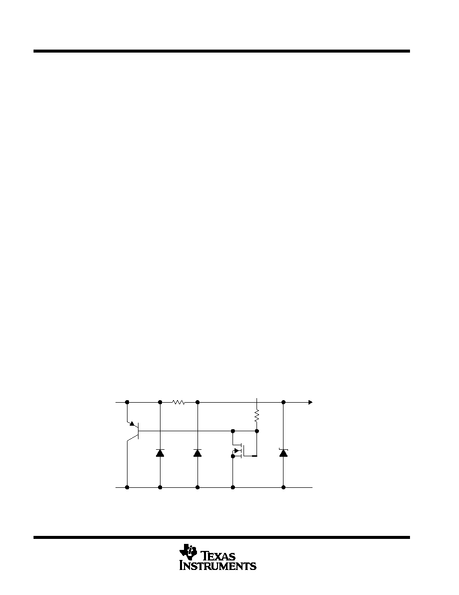
To overcome this limitation, TI design engineers developed the patented ESD-protection circuit shown in
Figure 4. This circuit can withstand several successive 1-kV ESD pulses, while reducing or eliminating leakage
currents that may be drawn through the input pins. A more detailed discussion of the operation of TI’s
ESD-protection circuit is presented on the next page.
All input an output pins of LinCMOS and Advanced LinCMOS products have associated ESD-protection
circuitry that undergoes qualification testing to withstand 1000 V discharged from a 100-pF capacitor through
a 1500-
resistor (human body model) and 200 V from a 100-pF capacitor with no current-limiting resistor
(charged device model). These tests simulate both operator and machine handling of devices during normal
test and assembly operations.
D1
D2
Q2
R2
D3
Q1
R1
VDD
To Protected Circuit
Input
VSS
Figure 4. LinCMOS ESD-Protection Schematic
相關(guān)PDF資料 |
PDF描述 |
|---|---|
| 5962-8765901CA | QUAD COMPARATOR, 10000 uV OFFSET-MAX, 650 ns RESPONSE TIME, CDIP14 |
| 5962-87659022A | QUAD COMPARATOR, 10000 uV OFFSET-MAX, 2500 ns RESPONSE TIME, CQCC20 |
| 5962-8765902CA | QUAD COMPARATOR, 10000 uV OFFSET-MAX, 2500 ns RESPONSE TIME, CDIP14 |
| 5962-9555001NXD | QUAD COMPARATOR, 10000 uV OFFSET-MAX, CDSO14 |
| 5962-9555001NXDR | QUAD COMPARATOR, 10000 uV OFFSET-MAX, 2500 ns RESPONSE TIME, PDSO14 |
相關(guān)代理商/技術(shù)參數(shù) |
參數(shù)描述 |
|---|---|
| 59628765901CA | 制造商:TI 功能描述:* |
| 5962-8765901CA | 制造商:Texas Instruments 功能描述:Comparator Quad 制造商:Rochester Electronics LLC 功能描述:- Bulk 制造商:Texas Instruments 功能描述:COMPARATOR QUAD 8V/16V 14CDIP - Rail/Tube |
| 5962-87659022A | 制造商:Texas Instruments 功能描述:Comparator Quad 16V 20-Pin LCCC Tube 制造商:Texas Instruments 功能描述:COMPARATOR QUAD 16V 20LCCC - Rail/Tube |
| 5962-8765902CA | 制造商:Texas Instruments 功能描述:Comparator Quad 16V 14-Pin CDIP Tube |
| 5962-8766001PA | 功能描述:功率驅(qū)動(dòng)器IC Dual-Power MOSFET Driver RoHS:否 制造商:Micrel 產(chǎn)品:MOSFET Gate Drivers 類型:Low Cost High or Low Side MOSFET Driver 上升時(shí)間: 下降時(shí)間: 電源電壓-最大:30 V 電源電壓-最小:2.75 V 電源電流: 最大功率耗散: 最大工作溫度:+ 85 C 安裝風(fēng)格:SMD/SMT 封裝 / 箱體:SOIC-8 封裝:Tube |
發(fā)布緊急采購,3分鐘左右您將得到回復(fù)。