- 您現(xiàn)在的位置:買賣IC網(wǎng) > PDF目錄67328 > 5962-8967602XX (CIRRUS LOGIC INC) 1-CH 16-BIT SUCCESSIVE APPROXIMATION ADC, SERIAL/PARALLEL ACCESS, CQCC44 PDF資料下載
參數(shù)資料
| 型號: | 5962-8967602XX |
| 廠商: | CIRRUS LOGIC INC |
| 元件分類: | ADC |
| 英文描述: | 1-CH 16-BIT SUCCESSIVE APPROXIMATION ADC, SERIAL/PARALLEL ACCESS, CQCC44 |
| 封裝: | CERAMIC, LCC-44 |
| 文件頁數(shù): | 10/50頁 |
| 文件大小: | 520K |
| 代理商: | 5962-8967602XX |
第1頁第2頁第3頁第4頁第5頁第6頁第7頁第8頁第9頁當(dāng)前第10頁第11頁第12頁第13頁第14頁第15頁第16頁第17頁第18頁第19頁第20頁第21頁第22頁第23頁第24頁第25頁第26頁第27頁第28頁第29頁第30頁第31頁第32頁第33頁第34頁第35頁第36頁第37頁第38頁第39頁第40頁第41頁第42頁第43頁第44頁第45頁第46頁第47頁第48頁第49頁第50頁

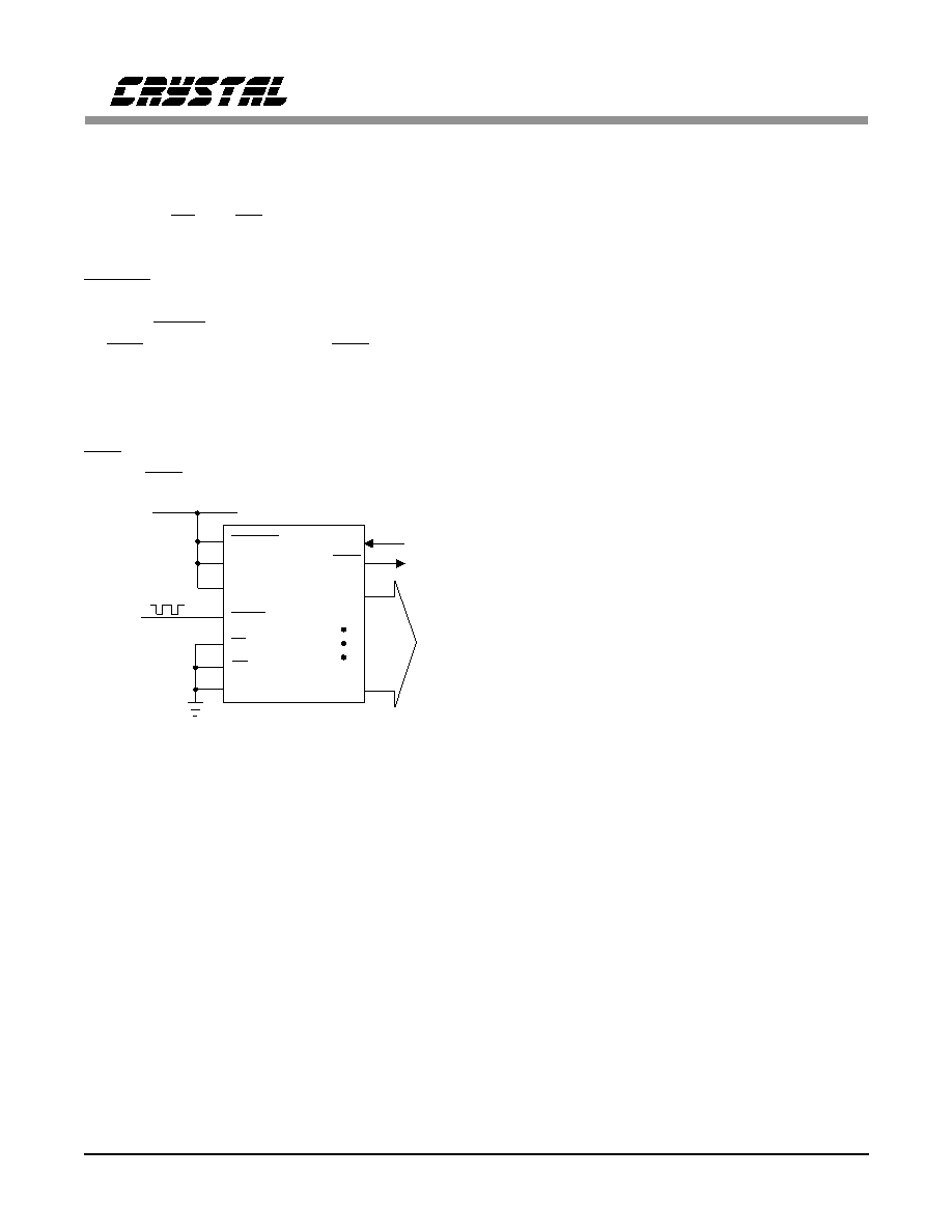
Microprocessor Independent Operation
The CS5012A/14/16 can be operated in a stand-
alone mode independent of intelligent control. In
this mode, CS and RD are hard-wired low. This
permanently enables the 3-state output buffers
and allows transparent latch inputs (CAL and
INTRLV) to be active. A free-running condition
is established when BW is tied high, CAL is tied
low, and HOLD is continually strobed low or tied
to EOT. The CS5012A/14/16’s EOC output can
be used to externally latch the output data if de-
sired. With CS and RD hard-wired low, EOC will
strobe low for four CLKIN cycles after each con-
version. Data will be unstable up to 100 ns after
EOC falls, so it should be latched on the rising
edge of EOC.
Serial Output
All successive-approximation A/D converters de-
rive their digital output serially starting with the
MSB. The CS5012A/14/16 present each bit to the
SDATA pin four CLKIN cycles after it is derived
and can be latched using the serial clock output,
SCLK. Just subsequent to each bit decision
SCLK will fall and return high once the bit infor-
mation on SDATA has stabilized. Thus, the rising
edge of the SCLK output should be used to clock
the data from the CS5012A/14/16 (See Figure 9).
ANALOG CIRCUIT CONNECTIONS
Most popular successive-approximation A/D con-
verters generate dynamic loads at their analog
connections. The CS5012A/14/16 internally buff-
er all analog inputs (AIN, VREF, and AGND) to
ease the demands placed on external circuitry.
However, accurate system operation still requires
careful attention to details at the design stage re-
garding source impedances as well as grounding
and decoupling schemes.
Reference Considerations
An application note titled "Voltage References for
the CS501X Series of A/D Converters" is avail-
able for the CS5012A/14/16. In addition to
working through a reference circuit design exam-
ple, it offers several built-and-tested reference
circuits.
During conversion, each capacitor of the cali-
brated capacitor array is switched between VREF
and AGND in a manner determined by the suc-
cessive-approximation algorithm. The charging
and discharging of the array results in a current
load at the reference. The CS5012A/14/16 in-
clude an internal buffer amplifier to minimize the
external reference circuit’s drive requirement and
preserve the reference’s integrity. Whenever the
array is switched during conversion, the buffer is
used to pre-charge the array thereby providing
the bulk of the necessary charge. The appropriate
array capacitors are then switched to the unbuf-
fered VREF pin to avoid any errors due to offsets
and/or noise in the buffer.
The external reference circuitry need only pro-
vide the residual charge required to fully charge
the array after pre-charging from the buffer. This
creates an ac current load as the CS5012A/14/16
sequence through conversions. The reference cir-
cuitry must have a low enough output impedance
to drive the requisite current without changing its
output voltage significantly. As the analog input
signal varies, the switching sequence of the inter-
nal capacitor array changes. The current load on
the external reference circuitry thus varies in re-
sponse with the analog input. Therefore, the
external reference must not exhibit significant
BW
CAL
RST
Reset
A0
CS
HOLD
+5V
Sampling
Clock
RD
D4
D15
Data
Out
12-Bit
EOC
Latching
Output
INTRLV
CS5012A
CS5014
CS5016
Figure 8. Microprocessor-Independent Connections
CS5012A, CS5014, CS5016
18
DS14F6
相關(guān)PDF資料 |
PDF描述 |
|---|---|
| 5962-8967402QX | 1-CH 14-BIT SUCCESSIVE APPROXIMATION ADC, SERIAL/PARALLEL ACCESS, CDIP40 |
| 5962-8967901XX | 1-CH 12-BIT SUCCESSIVE APPROXIMATION ADC, SERIAL/PARALLEL ACCESS, CQCC44 |
| 5962-8967402XX | 1-CH 14-BIT SUCCESSIVE APPROXIMATION ADC, SERIAL/PARALLEL ACCESS, CQCC44 |
| 5962-8967401QX | 1-CH 14-BIT SUCCESSIVE APPROXIMATION ADC, SERIAL/PARALLEL ACCESS, CDIP40 |
| 5962-8967401XX | 1-CH 14-BIT SUCCESSIVE APPROXIMATION ADC, SERIAL/PARALLEL ACCESS, CQCC44 |
相關(guān)代理商/技術(shù)參數(shù) |
參數(shù)描述 |
|---|---|
| 5962-8967701CA | 制造商:Linear Technology 功能描述:AMPLIFIER-OP AMP 制造商:Texas Instruments 功能描述:OP Amp Quad GP ±22V/44V 14-Pin CDIP Tube 制造商:Texas Instruments 功能描述:OP AMP QUAD GP 22V/44V 14CDIP - Rail/Tube 制造商:Texas Instruments 功能描述:LT1014AMJB QUAD PREC OP AMP |
| 5962-8967702CA | 制造商:Texas Instruments 功能描述:OP Amp Quad GP ±22V/44V 14-Pin CDIP Tube 制造商:Texas Instruments 功能描述:OP AMP QUAD GP 22V/44V 14CDIP - Rail/Tube |
| 5962-8967801XA | 制造商:Rochester Electronics LLC 功能描述:- Bulk 制造商:Analog Devices 功能描述: |
| 5962-8967802XA | 制造商:Rochester Electronics LLC 功能描述:8-BIT QUAD MULT DAC IC - Bulk 制造商:Analog Devices 功能描述: |
| 5962-8967901XC | 制造商:SEI 功能描述: |
發(fā)布緊急采購,3分鐘左右您將得到回復(fù)。